Technical Library | 2023-03-16 18:51:43.0
Conductive anodic filament (CAF) formation was first reported in 1976.1 This electrochemical failure mode of electronic substrates involves the growth of a copper containing filament subsurface along the epoxy-glass interface, from anode to cathode. Despite the projected lifetime reduction due to CAF, field failures were not identified in the 1980s. Recently, however, field failures of critical equipment have been reported.2 A thorough understanding of the nature of CAF is needed in order to prevent this catastrophic failure from affecting electronic assemblies in the future. Such an understanding requires a comprehensive evaluation of the factors that enhance CAF formation. These factors can be grouped into two types: (1) internal variables and (2) external influences. Internal variables include the composition of the circuit board material, and the conductor metallization and configuration (i.e. via to via, via to surface conductor or surface conductors to surface conductors). External influences can be due to (1) production and (2) storage and use. During production, the flux or hot air solder leveling (HASL) fluid choice, number and severity of temperature cycles, and the method of cleaning may influence CAF resistance. During storage and use, the principal concern is moisture uptake resulting from the ambient humidity. This paper will report on the relationship between these various factors and the formation of CAF. Specifically, we will explore the influences of printed wiring board (PWB) substrate choice as well as the influence of the soldering flux and HASL fluid choices. Due to the ever-increasing circuit density of electronic assemblies, CAF field failures are expected to increase unless careful attention is focused on material and processing choices.

Bicheng provides R&D, high-tech, IT research companies and organizations large or small with high frequency RF/microwave PCB's. Technical parameters: *NPTH and PTH( 20 um) *Thermal stress: 288C/10sec *Permitivity: ER2.1-1
Bicheng provides impedance controlled PCB's for R&D, high-tech, IT research companies and organizations, large or small. Technical parameters *Controlled dielectric *Controlled impedance *Design coupons *Test coupons *Po
Bicheng provides RD, high-tech, IT research companies and organizations, large or small with high quality bare PCB's PCB Products & Services * FR-4, High TG170, High CTI 600V * MCPCB, 1W/mk- 3W/mk * High speed
We supply bare printed circuit boards provided to us by our offshore manufacturing partners. Our partners have been fully researched and carefully selected, and are ISO certified and UL-approved. Single-Sided board Double-sided board Multilayer
New Equipment | Solder Materials
A variety of printed circuit boards require protection of selected board areas during the Surface Finish or Assembly Process. A wide range of PEELABLE SOLDER MASKS, the SD 295X Series including the popular SD 2954 and SD 2955 provide such protection
New Equipment | Assembly Services
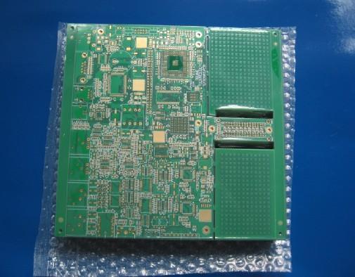
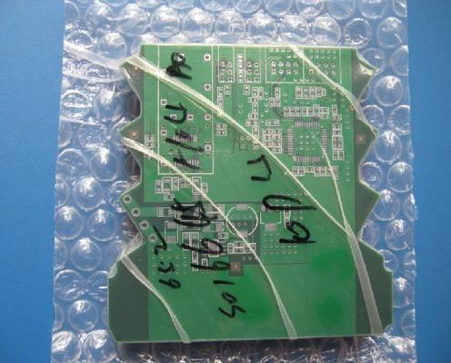
PCB process capability Base material: CM1, CM3, FR1, FR4, Metal based Layer: 1 to 24 layers Board thickness: 0.4mm to 3mm Copper thickness: 0.5oZ, 1oZ, 2oZ Min Copper thickness in hole: 0.02mm Max working size: 400*610mm Surface finishing: HAS
.jpg)
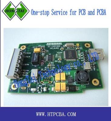
pcb assembly,pcb manufacture,printed board pbc Industrial Control Interface Board PCBA GTA-002 Catalog:pcb, pcb assembly,pcb manufacture, printed circuit board, pcb supply, pcb boards, electrical.suppliers. Raw Material: FR4 Finish: ENIG/ OSP/ H
Manufacture capability Layers: 1-16 layers Materials: CEM1, CEM3, Teflon, Rogers,FR-4, High Tg FR-4, Aluminum Base, Halogen Free Max. Board Size: 510*1200mm Material: RoHS Directive-compliant PCB thickness: 1.6 ±0.1mm Out Layer Copper Thickn
, FR-4 Tg170, ENIG.jpg)
New Equipment | Fabrication Services
High-density integration (HDI) technology enables the miniaturization of end product design while meeting higher standards of electronic performance and efficiency. Eastech has been focusing on high precision circuit board, continuously investing in


