Agilent Technologies, Inc.

World's premier measurement company, providing the critical tools and technologies that sense, measure, and interpret the physical and biological world.
When measurement matters, engineers, scientists, manufacturers, businesses, researchers, and government agencies rely on Agilent tools and solutions. From home entertainment to homeland security, from food safety to network reliability, and from communicating wirelessly to discovering the genetic basis of disease, Agilent provides the measurement capabilities that make our world more productive and a safer, healthier, more enjoyable place to live.
Agilent is committed to providing innovative measurement solutions that enable our customers and partners - the leaders in their fields - to deliver the products and services that make a measurable difference in the lives of people everywhere. With a singular focus on measurement, Agilent helps:
- Test more than half of the world's 1.13 billion cell phones
- Equip more than 200 communications service providers
- Advance next-generation integrated voice, video and data
- Analyze the causes and cures for disease
- Enable the military to be more flexible, mobile and reliable
- Make the world more safe and secure from crime and drugs
- Aid the discovery and quality of medicines
- Keep our air, water, soil and food clean and safe
Electronic Measurement
Agilent's electronic measurement business provides standard and customized electronic measurement instruments and systems, monitoring, management and optimization tools for communications networks and services, software design tools and related services that are used in the design, development, manufacture, installation, deployment and operation of electronics equipment and communications networks and services.
Agilent Technologies, Inc. Postings
3 products »
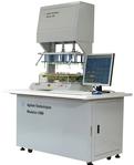
Medalist i1000D In-Circuit Test System
The Agilent Medalist i1000 in-circuit test (ICT) system is a low-cost in-circuit test solution which now comes with digital testing capabilities while maintaining its original low-cost fixture solution. The Medalist i1000 in-circui...
Agilent Medalist SP50 Series 3 - SPI
Automated 3D paste inspection for print process characterization, control and early defect prevention Best-in-class shadow free 3D paste measurement from the world’s leader in test and measurement. The Medalist SP50 Series 3...
In-circuit Test System - Medalist i3070
Improve both board test coverage and test throughput at in-circuit test with i3070 and i1000D ICT systems that offer one of the best ROICs available in the market today. The Medalist i3070, the next generation In-Circuit Test Syste...
7 technical articles »
Good Product Quality Comes From Good Design for Test Strategies
Dec 17, 2015 | Adrian Cheong
Product quality can be improved through proper application of design for test (DFT) strategies. With today's shrinking product sizes and increasing functionality, it is difficult to get good test coverage of loaded printed circuit boards due to the loss of test access. Advances in test techniques, such as boundary scan, help to recover this loss of test coverage. However, many of these test techniques need to be designed into the product to be effective.
This paper will discuss how to maximize the benefits of boundary scan test, including specific examples of how designers should select the right component, connect multiple boundary scan components in chains, add test access to the boundary scan TAP ports, etc. A discussion of DFT guidelines for PCB layout designers is also included. Finally, this paper will include a description of some advanced test methods used in in-circuit tests, such as vectorless test and special probing methods, which are implemented to improve test coverage on printed circuit boards with limited test access....
Pad Cratering Susceptibility Testing with Acoustic Emission
Aug 13, 2015 | Wong Boon San, Julie Silk; Agilent Technologies | Richard Nordstrom, Ph.D.; Acoustic Technology Group,
Pad cratering has become more prevalent with the switch to lead free solders and lead free compatible laminates. This mainly is due to the use of higher reflow temperature, stiffer Pb-free solder alloys, and the more brittle Pb-free compatible laminates. However, pad cratering is difficult to detect by monitoring electric resistance since pad cratering initiates before an electrical failure occurs.
Several methods have been developed to evaluate laminate materials' resistance to pad cratering. Pad-solder level tests include ball shear, ball pull and pin pull. The detailed methods for ball shear, ball pull, and pin pull testing are documented in an industry standard IPC-9708. Bansal, et al. proposed to use acoustic emission (AE) sensors to detect pad cratering during four-point bend test. Currently there is an industry-working group working on test guidelines for acoustic emission measurement during mechanical testing....
Aug 29, 2013 | Mike Powers, Jianbiao Pan, Julie Silk, Patrick Hyland
Au over Ni on Cu is a widely used printed circuit board (PCB) surface finish, under bump metallization (UBM), and component lead metallization. It is generally accepted that less than 3 wt.% Au in Sn-Pb solder joints inhibits formation of detrimental intermetallic compounds (IMC). However, the critical limit for Au content in Pb-free solder joints is not well established. Three surface-mount package platforms, one with a matte Sn surface finish and the others with Ni/Au finish, were soldered to Ni/Au-finished PCB using Sn-3.0Ag 0.5Cu (SAC305) solder, in a realistic manufacturing setting. The assembled boards were divided into three groups: one without any thermal treatment, one subjected to isothermal aging at 125°C for 30 days, and the third group aged at 125°C for 56 days... ...
Boundary Scan Advanced Diagnostic Methods
Feb 14, 2013 | Christopher Cain
Boundary-scan (1149.1) technology was originally developed to provide a far easier method to perform digital DC testing to detect intra-IC interconnect assembly faults, such as solder shorts and opens. Today's advanced IC technology now includes high-speed differential interfaces that include AC or DC coupling components loaded on the printed circuit assembly. Simple stuck-at-high/low test methods are not sufficient to detect all assembly fault conditions, which includes shorts, opens and missing components. Improved diagnostics requires detailed circuit analysis, predictive assembly fault simulation and more complex testing to isolate and accurately detect all possible assembly faults... First published in the 2012 IPC APEX EXPO technical conference proceedings...
The Morphology Evolution and Voiding of Solder Joints on QFN Central Pads with a Ni/Au Finish
Oct 18, 2012 | Julie Silk, Jianbiao Pan, Mike Powers
First published in the 2012 IPC APEX EXPO technical conference proceedings. In this paper, we report on a comprehensive study regarding the morphology evolution and voiding of SnAgCu solder joints on the central pad of two different packages – QFN and an Agilent package called TOPS – on PCBs with a Ni/Au surface finish....
Evaluation of Laminates in Pb-free HASL Process and Pb-free Assembly Environment
Sep 20, 2012 | Khaw Mei Ming, Andrey Lee
First published in the 2012 IPC APEX EXPO technical conference proceedings. An evaluation of four FR4 laminates in commonly used stack-ups was done to determine their survivability for the Pb-free HASL process followed by a worst case Pb-free manufacturin...
Thermal Cycle Reliability Study of Vapor Phase BGA Solder Joints
Sep 13, 2012 | Ward Gatza; Agilent Technologies, Inc., Tom Evans; Thomas C. Evans Consulting
First published in the 2012 IPC APEX EXPO technical conference proceedings. Prior to committing production boards to vapor phase soldering, we performed an evaluation to assess reliability and evaluate the vacuum soldering option. The reliability of vapor...
96 news releases »
Agilent Technologies Reveals Name of Electronic Measurement Spin-Off Company
![]() Jan 08, 2014 | Agilent Technologies revealed the name of the electronic measurement company it expects to spin off in early November 2014 as Keysight Technologies.
Jan 08, 2014 | Agilent Technologies revealed the name of the electronic measurement company it expects to spin off in early November 2014 as Keysight Technologies.
Agilent gets serious about JTAG test
![]() Jun 29, 2010 | Agilent Technologies’ interest in boundary scan test support grows with its second JTAG test systems move in a month.
Jun 29, 2010 | Agilent Technologies’ interest in boundary scan test support grows with its second JTAG test systems move in a month.
Agilent Technologies' Digital Measurement Forum Focuses on Trends Influencing Future of Industry
![]() Jun 20, 2009 | Agilent Technologies Inc. (NYSE: A) today kicked off its Agilent Digital Measurement Forum (ADMF) in Seoul, Korea. The annual forum, which brings together local and global industry leaders to address all digital-related measurement solutions from consumer electronics to high-speed digital design, will be held in six countries in the Asia-Pacific region from June 18 to July 16. Partners and collaborators such as Xilinx, The MathWorks and Microchip Technology are participating in the forum.
Jun 20, 2009 | Agilent Technologies Inc. (NYSE: A) today kicked off its Agilent Digital Measurement Forum (ADMF) in Seoul, Korea. The annual forum, which brings together local and global industry leaders to address all digital-related measurement solutions from consumer electronics to high-speed digital design, will be held in six countries in the Asia-Pacific region from June 18 to July 16. Partners and collaborators such as Xilinx, The MathWorks and Microchip Technology are participating in the forum.
Agilent Technologies Presents the 2009 Aerospace Defense Symposium "Focus Where it Counts"
![]() Feb 15, 2009 | Agilent's Aerospace and Defense Symposium begins a two-month U.S. tour on February 23, 2009. The symposium provides presentations and demonstrations on how to combine design tools with cutting edge test solutions to help you build greater assurance in system readiness so you can focus on today's challenging missions.
Feb 15, 2009 | Agilent's Aerospace and Defense Symposium begins a two-month U.S. tour on February 23, 2009. The symposium provides presentations and demonstrations on how to combine design tools with cutting edge test solutions to help you build greater assurance in system readiness so you can focus on today's challenging missions.
Agilent Technologies' New Solder Paste Inspection System Available Feb. 15
![]() Jan 21, 2009 | The Medalist SP50 Series 3 Dual Laser SPI System Offers Defect Coverage Down to 01005 Level
Jan 21, 2009 | The Medalist SP50 Series 3 Dual Laser SPI System Offers Defect Coverage Down to 01005 Level
Agilent Technologies Displays Comprehensive Femtocell Testing Capability
![]() Dec 06, 2008 | Agilent Technologies Inc. (NYSE: A) today announced it is demonstrating its comprehensive femtocell design and test capabilities here at the Femtocells USA event, Dec. 1-3. Included in its offering is the first 3GPP LTE femtocell test system used to test reference design.
Dec 06, 2008 | Agilent Technologies Inc. (NYSE: A) today announced it is demonstrating its comprehensive femtocell design and test capabilities here at the Femtocells USA event, Dec. 1-3. Included in its offering is the first 3GPP LTE femtocell test system used to test reference design.
![]() Nov 19, 2008 | SANTA CLARA, Calif., and SAN JOSE, Calif., Nov. 18, 2008
Nov 19, 2008 | SANTA CLARA, Calif., and SAN JOSE, Calif., Nov. 18, 2008
Agilent Technologies to Present Advances in Limited Access Test Solutions at International Test Week
![]() Oct 01, 2008 | Agilent's R&D scientists for In-Circuit Test solutions will be presenting at various sessions throughout the conference.
Oct 01, 2008 | Agilent's R&D scientists for In-Circuit Test solutions will be presenting at various sessions throughout the conference.
Agilent Technologies, Altron Inc. Announce Altron's Selection of Agilent Medalist sj5000 AOI System
![]() Sep 24, 2008 | sj5000 Selected
Sep 24, 2008 | sj5000 Selected
![]() Sep 08, 2008 | Agilent Technologies Inc. (NYSE: A) today introduced a new member of the function/arbitrary waveform family that delivers high-quality waveforms at an economical price. For design development and test engineers who need lower-frequency signals without sacrificing accuracy, this new instrument easily generates the waveforms needed for bench and system applications.
Sep 08, 2008 | Agilent Technologies Inc. (NYSE: A) today introduced a new member of the function/arbitrary waveform family that delivers high-quality waveforms at an economical price. For design development and test engineers who need lower-frequency signals without sacrificing accuracy, this new instrument easily generates the waveforms needed for bench and system applications.


