High-density multi-layer PCB with 3 Mils Minimum Line Width
Company Information:
Name: |
High-density multi-layer PCB with 3 Mils Minimum Line Width |
Category: |
|
Offered by: |
|
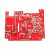
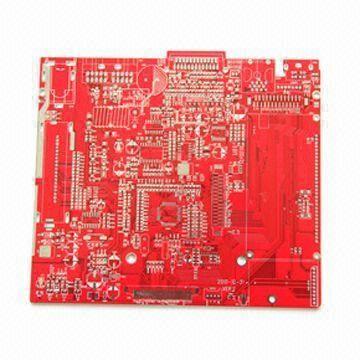
High-density multi-layer PCB with 3 Mils Minimum Line Width Description:
Material: FR-4 Tg 170/1.6mm/2oz Layer coverage: 6 Size: 107 x 82mm Minimum line width/space: 3 mils Minimum hole size: 0.15mm Application: locating devices Routed profile: ±0.10mm Scored edge: ±0.30mm Finished hole (plated): ±0.075mm Finished hole drill (non-plated): ±0.05mm Hole position deviation: ±0.075mm Twist and bent: 0.75% Insulation resistance: >1,012 (normal) Electric strength: >1.3kV/mm Thermal stress: 288°C, 20 seconds Testing voltage: 50 to 300V Packing: vacuum packing for PCB, and good condition outer boxesHigh-density multi-layer PCB with 3 Mils Minimum Line Width was added in Jan 2011
High-density multi-layer PCB with 3 Mils Minimum Line Width has been viewed 427 times
2 More Products from Shenzhen Linghangda Electronic Co.,Ltd :