Photo Stencil LLC
Photo Stencil provides high-performance stencils, squeegee blades, thick film and metal mask screens and tooling for the surface mount technology (SMT) assembly, solar, and semiconductor industries.
Photo Stencil, LLC provides high-performance stencils, squeegee blades, thick film and metal mask screens and tooling for the surface mount technology (SMT) assembly, solar, and semiconductor industries. Its innovations include the patented AMTX E-FAB® electroform stencils, high-performance, proprietary NicAlloy™, NicAlloy-XT™, laser-cut, and chemetch stencils, and patented electroformed E-Blade® squeegee blade. Stencil design support and customer-specific design libraries are also provided. Founded in 1979, Photo Stencil is headquartered in Colorado Springs and has manufacturing facilities in Mexico and Malaysia. For more information follow us on www.linkedin.com/company/Photo-Stencil-LLC, visit www.photostencil.com, or email info@photostencil.com.
Photo Stencil LLC Postings
2 products »
Electroformed Stencils - Hard Nickel NiEX™
NiEX™ electroformed stencils use the same proprietary process as our market leading AMTX™ stencils. The NiEX™ stencil has a higher Knoop Hardness (HK) than our standard AMTX product for those very thin less than...
Laser Fab, NiPlate™, NanoCoat™. NicAlloy-XT™ stencils are the premier laser-cut stencils in the industry. Beginning life as a laser-cut stencil, followed by a secondary process utilizing Photo Stencil’s own prop...
7 technical articles »
Step Stencil design when 01005 and 0.3mm pitch uBGA's coexist with RF Shields
Jul 25, 2023 | William E. Coleman Ph.D.
Some of the new handheld communication devices offer real challenges to the paste printing process. Normally, there are very small devices like 01005 chip components as well as 0.3 mm pitch uBGA along with other devices that require higher deposits of solder paste. Surface mount connectors or RF shields with coplanarity issues fall into this category. Aperture sizes for the small devices require a stencil thickness in the 50 to 75 um (2-3 mils) range for effective paste transfer whereas the RF shield and SMT connector would like at least 150 um (6 mils) paste height. Spacing is too small to use normal step stencils. This paper will explore a different type of step stencil for this application; a "Two-Print Stencil Process" step stencil. Here is a brief description of a "Two-Print Stencil Process". A 50 to 75 um (2-3 mils) stencil is used to print solder paste for the 01005, 0.3 mm pitch uBGA and other fine pitch components. While this paste is still wet a second in-line stencil printer is used to print all other components using a second thicker stencil. This second stencil has relief pockets on the contact side of the stencil any paste was printed with the first stencil. Design guidelines for minimum keep-out distances between the relief step, the fine pitch apertures, and the RF Shields apertures as well relief pocket height clearance of the paste printed by the first print stencil will be provided....
Stencil Options for Printing Solder Paste for .3 Mm CSP's and 01005 Chip Components
Jul 25, 2023 | William E. Coleman Ph.D. , Chris Anglin
Printing solder paste for very small components like .3mm pitch CSP's and 01005 Chip Components is a challenge for the printing process when other larger components like RF shields, SMT Connectors, and large chip or resistor components are also present on the PCB. The smaller components require a stencil thickness typically of 3 mils (75u) to keep the Area Ratio greater than .55 for good paste transfer efficiency. The larger components require either more solder paste height or volume, thus a stencil thickness in the range of 4 to 5 mils (100 to 125u). This paper will explore two stencil solutions to solve this dilemma. The first is a "Two Print Stencil" option where the small component apertures are printed with a thin stencil and the larger components with a thicker stencil with relief pockets for the first print. Successful prints with Keep-Outs as small as 15 mils (400u) will be demonstrated. The second solution is a stencil technology that will provide good paste transfer efficiency for Area Ratio's below .5. In this case a thicker stencil can be utilized to print all components. Paste transfer results for several different stencil types including Laser-Cut Fine Grain stainless steel, Laser-Cut stainless steel with and w/o PTFE Teflon coating, AMTX E-FAB with and w/o PTFE coating for Area Ratios ranging from .4 up to .69....
Stencil Print solutions for Advance Packaging Applications
Jul 25, 2023 | Phani Vallabhajosyula, PhD
This paper address two significant applications of stencils in advance packaging field: 1. Ultra-Thin stencils for miniature component (0201m) assembly; 2. Deep Cavity stencils for embedded (open cavity) packaging. As the world of electronics continues to evolve with focus on smaller, lighter, faster, and feature-enhanced high- performing electronic products, so are the requirement for complex stencils to assemble such components. These stencil thicknesses start from less than 25um with apertures as small as 60um (or less). Step stencils are used when varying stencil thicknesses are required to print into cavities or on elevated surfaces or to provide relief for certain features on a board. In the early days of SMT assembly, step stencils were used to reduce the stencil thickness for 25 mil pitch leaded device apertures. Thick metal stencils that have both relief-etch pockets and reservoir step pockets are very useful for paste reservoir printing. Electroform Step-Up Stencils for ceramic BGA's and RF Shields are a good solution to achieve additional solder paste height on the pads of these components as well as providing exceptional paste transfer for smaller components like uBGAs and 0201s. As the components are getting smaller, for example 0201m, or as the available real estate for component placement on a board is getting smaller – finer is the aperture size and the pitch on the stencils. Aggressive distances from step wall to aperture are also required. Ultra-thin stencils with thicknesses in the order of 15um-40um with steps of 15um are used to obtain desired print volumes. Stencils with thickness to this order can be potential tools even to print for RDLs in the package....
Stencil Design For Mixed Technology Through-Hole / Smt Placement And Reflow
Jun 12, 2023 | William E. Coleman, Denis Jean, Julie Bradbury
This paper will review stencil design requirements for printing solder paste around and in through-hole pads / openings. There is much interest in this procedure since full implementation allows the placement of both through-hole components as well as SMD's and the subsequent reflow of both simultaneously. This in turn eliminates the need to wave solder or hand solder through-hole components....
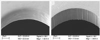
Print Performance Studies Comparing Electroform and Laser-Cut Stencils
Nov 05, 2015 | Rachel Miller Short, William E. Coleman Ph.D.; Photo Stencil | Joseph Perault; Parmi.
There has been recent activity and interest in Laser-Cut Electroform blank foils as an alternative to normal Electroform stencils. The present study will investigate and compare the print performance in terms of % paste transfer as well the dispersion in paste transfer volume for a variety of Electroform and Laser-Cut stencils with and without post processing treatments. Side wall quality will also be investigated in detail. A Jabil solder paste qualification test board will be used as the PCB test vehicle....
Electroformed vs. Laser-cut: A Stencil Performance Study
Jan 11, 2013 | By Michael R. Burgess and William E. Coleman, Ph.D., Photo Stencil
There have been claims in the industry that laser-cut electroformed nickel foil blanks provide stencil print performance comparable to electroformed stencils. A study was established to measure the quantitative differences in performance between the two during an independent lab study....
Stencil Printing of Small Apertures
Oct 25, 2012 | William E. Coleman Ph.D.
First published in the 2012 IPC APEX EXPO technical conference proceedings. This paper will examine stencil technologies (including Laser and Electroform), Aperture Wall coatings (including Nickel-Teflon coatings and Nano-coatings), and how these parameters influence paste transfer for miniature devices with Area Ratios less than the standard recommended lower limit of .5. A matrix of print tests will be utilized to compare paste transfer and measure the effectiveness of the different stencil configurations. Area Ratios ranging from .32 to .68 will be investigated....
4 news releases »
 Mar 10, 2016 | Photo Stencil will showcase advanced stencils for printing the most demanding PCB and semiconductor packaging designs at IPC APEX 2016, Las Vegas, CO, March 15-17, 2016, in booth #825.

Photo Stencil Sells Guadalajara, Mexico Laser Stencil Business to Management Team
Dec 13, 2015 | Photo Stencil announces that it has sold the Photo Stencil business in Guadalajara, Mexico to the facility's management team, Francisco Lujano and Armando Berumen. Photo Stencil's Mexico facility produces laser-cut stencils and will continue to sell both the laser-cut stencils they manufacture and electroform stencils that will be made by Photo Stencil in its new Golden, CO facility.

Oct 11, 2015 | Photo Stencil announces that Susan Holmes, VP engineering and customer service for Photo Stencil, will present the paper Stencil Design for Wafer Level Ball Drop and Flip Chip Assembly at the IWLPC during Session 10 on Wednesday, October 14, 2015, at 5:00 PM. The 12th Annual International Wafer-Level Packaging Conference and Tabletop Exhibition is being held at the Doubletree San Jose Airport Hotel, San Jose, CA.

Sep 30, 2013 | Free Session, Spotlight 4, October 16, 2013
from 9:30-11:00 AM