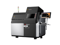
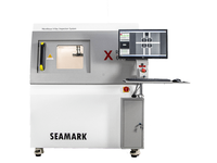
LED PCB X-Ray Inspection System X-1200
Company Information:

Name: |
LED PCB X-Ray Inspection System X-1200 |
Category: |
|
Offered by: |
|
LED PCB X-Ray Inspection System X-1200 Description:
LED PCB X-Ray Inspection System X-1200
- SMT /Semicon/Solar/Harness Connector/LED PCB (Special for LED 1200mm)
- High-definition image: Slanting/Bridge/Voids/Cold Solder/Bonding wire
- 90KV 5μm closed X-ray tube,with long life,maintenance in free
- 1.3 million high resolution digital flat panel detector
- Color image navigation, easy to use
- Automatic programming detection and automatic analysis NG or OK
Application
1) Defect inspection in IC packaging, e.g.: layer separation, cracking, void, and line integrity.
2) Measuring chip size, measuring line curvature, measuring the proportion of solder area of components.
3) Possible defects in PCB manufacturing processes, e.g.: misalignment, solder bridge and open.
4) SMT solder short, cold solder, component shifted, solder insufficient, solder void inspection and measurement.
5) Defect inspection of open, short or abnormal connections that may occur in automotive wiring harnesses and connectors.
6) Inner rupture or hollow inspection in plastic or metal.
7) Battery stacking uniformity, electrode welding inspection.
8) Seed, biological material inspection etc.


LED PCB X-Ray Inspection System X-1200 was added in Sep 2018
LED PCB X-Ray Inspection System X-1200 has been viewed 418 times
11 More Products from Seamark ZM Technology Group Co.,Ltd :