|
Proof Of Design a continuing column (saga) by The MoonMan
|
Installment 3: DFM/CE Design Development Phases
Sure, certain limitations are placed on travels wherever we go though they're certainly not so restrictive as space travel. When I journey into space (often, as you might assume), it is a different experience than down home on roads less traveled. Even though an incredible adventure, every possible safety and operational precaution must be in place and observed or the sense of it all, as do all senses, ends abruptly. Rules abound and apply to every activity.
Back down on earth, the adventure ends and reality returns where "civilization" begins. Ok, so it's unacceptable to be careless in your space suit or craft. If you puncture something (as when taking seriously a boss's suggestion), eternal freedom results and that's something I'm not remotely prepared to experience. Doubt I'll ever be. So, is there more or less freedom for earth bound mortals? It seems no matter where you go, there are rules - for our own good of course.
RULES? RULES? WE DON'T NEED NO STINKIN' RULES
I'm so damn tired of rules and all other such limitations placed on my freedom. We have too many as it is. Look at them all. Hell, you couldn't count them in a lifetime. How then could you obey them all? I mean, it's illegal even spit on a sidewalk or bug, if so inclined. I've never been a spitter - even while playing semi-pro baseball as all others around me practiced the craft often better than they played. Why, I wonder now, did some of them move up to the big's and not me? Hmmm - spituey! Still, I reserve the right to spit on a bug, though never a sidewalk (I do have some class). Damn rules anyway. I'll take my chances breaking some - doubtless without even knowing.
So why should I, of all people, want rules telling me how to design something? I can't explain it, having always been a "free-spirited" type. Even though I once sought discipline in the Marine Corps, I soon learned that type excess didn't always work well for me except when flying aircraft (after all, that's life & death stuff - much like playing in jungle settings). After my ever so positive experience in the "crotch", it was time to get loose. Excel at that I did. Even so, I do love the rules of designing product meeting specified requirements. What's wrong with this picture?
A little late to learn or care much about what's wrong with me - what about you all? I mean, everyone has to follow so many rules just to get components to "stick" to boards. Often it must be done in ways spiteful of design intent, and more often made up as you go (Steve "McGyver" Gregory, where have you gone?). Could we use fewer during manufacture if more or better rules were used during design phases?
From the questions and responses on the SMTnet forum, it is clear you all want more order in your lives, at least those working. Fewer hours spent correcting problems would make life better too, I suspect. I've never seen anyone write "I would rather do it wrong," or "why don't those designers give me a bad board to assemble because I'm tired of doing it right all the time?" Certainly, I've never ever seen anyone expressing happiness about doing it over and over when it could'a/should'a been done right the first time.
THINGS WE'VE ALL SEEN OR DONE OURSELVES
Maybe, because so few of us ever have experienced "just doing it - but doing it right," we want so much to experience the feeling at least once. Maybe, those having done it right before, but no longer, just can't quit looking for another opportunity. Maybe those doing it right, right now, just can't get enough so seek continuous improvement. Maybe, I'm full of it.
The reality is we are doing it better, for the most part, than ever before in this country. We're also doing it faster, while doing it better. And, don't bring up costs because no one can complain about the prices of new computers or parts though new car prices suck onward higher. Certainly, we are doing it better, faster, and cheaper than anyone else on the planet. However, of course, we take what we do all over the world to our credit and benefit realizing the lower costs. Aren't we wonderful? How about those Nike folks? Where are they now, anyway?
Naturally, it is only fair to mention "Emperor Gates'" (when will he buy a country?) comment about the car industry and how they should be doing it the same way as him so cars would become increasingly cheaper (by the way, I haven't seen lower prices for MS Office 2000). The auto industry's answer was sure, but customers wouldn't like restarting their cars when they so often quit running unexpectedly. So, there are some flies in the stew. They too could be eliminated through better DFM/CE efforts. What purpose do flies serve anyway?
Ok, so we're doing it better, faster, and cheaper. Is that reason to stop seeking improvement, or should we go for more? We, meaning us all, comprise the strongest industrial complex ever and, without a doubt, can do more of anything we wish or can even imagine. There are no limits but for those stinkin' rules. Is that so?
Very few among us can take pride in not having developed a business plan but having received millions in vulture capital anyway - because of a great idea or daddy's name. Sure, but it doesn't happen often. It is rare when money is risked on a venture unproven or without a plan, made up of clearly defined rules, telling exactly how something is going to get done - when, where, how, why, and by whom. Oh yes, don't forget rules about having to mortgage all belongings including wife and kids.
Investment types want, no - demand, from 10 to 20:1 return on their money within a clearly defined period (3 - 5 years is typical - why do you think they're rich and we're not?). Without this assurance, clearly stated in a business plan, they will not risk anything. Following the business plan, its successful implementation (measured by successful funding) and startup, comes organizational structuring.
It may not always seem so, and they may not always be clear, but rules tie it all together. Again, it's always a matter of who, what, when, where, why, and how. This always is true even in seemingly much less structured, "free spirited organizations." As "loosey goosey" as some startups appear (internet and software types come to mind first), try finding anyone not adhering to strict rules. They may be self-imposed (out of pride, dedication, greed, peer pressure, or compulsion), computer related (try writing code without rules), or deadline driven (drop dead leaps to mind) - but never money driven of course.
Just try running an SMT line without rules. All right, bad example. That happens everyday, but not for long if business and financial success really is a goal. I believe we all have horror stories to tell here especially concerning operators not following procedures, as but one example.
Ok, everyone knows all this stuff. By now you're asking where is this going, if your still reading, or if you ever started. If this stuff really turns you on, you might excitedly be asking what's next? Glad you asked.
Simply, product must be conceived, engineered, designed, produced, and accepted all according to rules. How does DFM/CE aid this process, and what does it take to get this part of the DFM/CE equation balanced? Let's take a look at various design phases while considering one very important - design rule development, and how it starts very early in the process.
DFM/CE DESIGN PHASES
Five major design phases are required to effect a design capable of being manufactured, proven, and accepted. Each phase requires CE, based on certain rules, before another phase begins. It also should be noted that using DFM/CE this way (the right way) improves design guidelines as progress is made. Then, rules may be developed from them during POD. The phases are:
CONCEPTUAL
The conceptual design phase begins when the program manager and/or responsible engineer receives requirements for a new project or program (as developed and indicated in this column's installment 2). It is during this phase a concept initially is developed as one thought capable of meeting rudimentary product requirements. Even so, during this phase, little thought may be given to manufacturing or quality requirements though more should and can be with a little experience.
This is a time for blocking out a diagram depicting and describing a product's form and basic functionality (again, as described in installment two). However, CE must be on the developer's mind before the next phase is started, and input should be sought from design guidelines while seeking brief conference with DFM/CE team members already appointed to the roster.
At this point, all the tools provided in installment two should be formulated for immediate use. Of particular importance, once the DFM/CE team is formalized, is the "PRODUCT MANUFACTURABILITY AUDIT CHECK LIST." It must find very early use as a tool to begin determining product and manufacturing process compatibility.
Using the audit checklist, the program manager invites DFM/CE team members to a meeting that's agenda primarily is focused on early product/process compatibility issues. It is at this time the team provides initial input as to whether the design concept is capable of being produced in each of the manufacturing processes currently known and available.
During this very early stage it is not possible to visualize all design or process requirements, but a baseline may be established. Over time, deviations and compromises will be realized and forthcoming. Now it is easy to track them, so things don't stray into an arena no one ever has entered. Once the checklist is initiated, it is possible to resume the conceptual phase while assuring traceability to its origin.
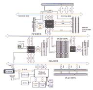
Design project input may be as simple as describing requirements for a personal computer, a network consisting of several, or components required therein. Again, output may consist of a simple block diagram showing all major product elements. It provides input directly to the schematic development phase with device design level selection considered after.
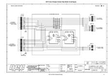
SCHEMATIC DEVELOPMENT
This phase requires creating a preliminary schematic for output to the next design phase. The schematic takes input as the basic block diagram to a higher detail level and provides graphic information concerning what comprises each block. Also, it must be concurrently developed to satisfy package requirements initially considered in the device selection phase following.
In a computer system, a graphics card - as a single block example, is detailed to a proposed component level including how each device is connected electrically. It provides no information about packages or device types and their mounting locations on the PCB, but thought always must be on them. This comes as part of concurrent device selection process. Again, this requires input from all team members to ensure more effective, efficient phase management through acceptance.
During initial schematic development, many important design considerations may be clarified and noted for early evolution to possible design rule status. This type thinking must start at the schematic level while using available internal or industry guidelines. This is not jumping ahead. It is concurrence at work. Therefore, it is not the responsibility of the EE alone to bear the burden though advice should be given and considered. The rest of the team provides input for earlier, quicker, better decision making during this phase instead of having to go through endless schematic level design reviews.
Note: I know of few organizations using this approach except for those doing highly advanced commercial or aerospace work. This is a target rich environment begging opportunity exploration. You can't start too early developing rules for earlier success.
Other issues may crop up early in CE discussions. They may involve device reliability or even solderability. Also, moisture or thermal requirements may be issues for early concurrent thinking as it may not be possible to use some plastic devices under either high moisture or temperature conditions. This may directly affect the EE's decisions on how to formulate an acceptable schematic as early as possible. It must be said again, it is not too soon during this phase to make these considerations and judgements.
Once packages or device types are selected from a qualified parts list (QPL), or approved vendor list (AVL), they may be placed on a preliminary bill of materials (BOM). This process may begin life during the schematic development phase to save even more time. After this, it becomes more clearly apparent which device or package types are best suited to design, manufacturing, and test processes. When the schematic phase, using DFM/CE to best advantage, is complete, the device selection phase begins and is made easier with additional CE having been effected during the schematic phase.
DEVICE SELECTION, PACKAGE, AND PACKAGING CONSIDERATION
This design phase provides more opportunity for DFM/CE. It is during this phase device selection and package/packaging considerations are made near final. Therefore, it is critical that concurrence is sought. Again, basic requirements were described in installments one and two. Now, the audit checklist really comes into play. Just as it was used for printed circuit board supplier evaluations, it is now used for components.
The DFM/CE team must be readily available for this particular program phase based on the time line as described in installment two. It must focus clearly on the quickly evolving design phases, now having a much more mature schematic than normally available. It is time to proceed with component selection process while concurrently considering package and design/product packaging requirements.
Again, at a minimum, the team must be composed of design, component, process, manufacturing, test, and quality engineering. Now, it also would be advisable to seek further management, marketing, and customer input to ensure focus is more clearly directed toward product expectations. These expectations have considerable impact on manufacturability as a function of how well this phase is managed. With additional team members, it is easier to maintain focus and not allow it to become side tracked.
Though form and fit requirements take a back seat to function, at this time, they must be considered as a function of Electro-mechanical packaging. If the customer or a market segment has provided some input about appearance, this is a place to start. If the design originates internally, there may be more freedom though limitations may arise as size constraints, ergonomics, safety, or other.
In any case, early packaging requirements can impact individual package choices. However, it is most important to consider how they will impact manufacturability and quality.
The team begins seriously considering choices about whether a certain device, and its package style, is suitable relative to the overall packaging design. This means evaluating whether a package is to be a through hole or surface mount type, as an example (size and space may be considerations here). Further, it becomes necessary to consider whether a SMT device would be a leaded type or BGA, as an example. These considerations must be effected for all packages and device types to be selected, and I bring this up now to save time and effort during this and subsequent phases.
During this phase, many more design considerations may be clarified based on initial work done during the schematic phase. This ensures early evolution to clearly defined design rule status using modified design guidelines mostly with focus on manufacturing requirements.
All new information must be verified for additional packaging requirements, as it is basic and must be considered while looking now at the whole assembly instead of the device package itself. In other words, it initially is possible to select a unique device type for top or bottom side mounting. Although, when other devices are selected for various mounting positions, it becomes necessary to balance the entire assembly package for design and manufacturability. Requirements include not attaching, as an example, BGA's on the assembly's bottom side - whenever possible. Instead, it may be necessary to use QFP's instead. As another example, if the schematic requires two ASIC's (possibly as BGA's though yet to be determined), consideration should now be made concerning their mounting locations (both top or bottom, or?)
With device selection made, based on package types and the overall package design, it is possible to assess impact on the design layout phase as well as verifying further the schematic integrity. With close CE, the next phase begins as the designer keeps in mind, or is reminded by the team, important rules developed partially in this phase.
DESIGN LAYOUT
The design layout phase is effected after the DFM/CE team has finished its preliminary device/package type selection process and other considerations made during the schematic development phase. Now, the devices may be "placed" on "surfaces" representing the proposed PCB. This is done using computer aided design (CAD) capabilities.
The designer is given input information as a proposed schematic. The schematic is "captured" electronically and converted into information useable in the CAD program so a component layout may be effected.
The designer has, in a database, a component library. The library probably has a majority of package types considered during the DFM/CE portion of the schematic development phase. It is clear some devices will not be there as they may just have been considered for the first time at the schematic phase. The DFM/CE team's role here is to work with the designer to make the best selections. This process takes place in scheduled meetings. If a new device type is required, it temporarily may be placed in the library based on information obtained from the device manufacturer data sheets. If the device is proven to work as specified, and the DFM/CE team agrees the device is acceptable, it may be placed permanently in the library.
Certain physical constraints are imposed on the product package size. This also is true of process constraints. In both cases, board sizes are limited to these constraints. This may make it difficult to place all the preliminarily selected devices (from the schematic phase and parts library) on either or both board sides. This again, is where the DFM/CE team focuses on the preliminary layout and how components impact design and manufacturability effectiveness.
Once all selected devices are placed considering schematic and physical requirements and constraints, respectively, the layout must be reviewed for manufacturability notwithstanding upcoming routing requirements. Again, if a device or package type/style is not suitable for a particular mounting location, it must be reconsidered as an alternate type or style. It also may become known that all the devices will not fit on the selected board size. In this event, it may be possible to find other components in smaller package sizes, or to combine some in a new ASIC's.
CE comes into play here too because certain manufacturing or performance issues may conflict. Other considerations must be made as well and will be detailed in emerging (from guidelines) design standards (rules). This phase's output is a completed and approved component layout ready for circuit routing.
DESIGN ROUTING
This phase concerns routing soon becoming PCB metal trace conductors on the board's surfaces whether single sided, double sided, or multilayered. This phase's input is a completed and concurrently approved design layout with all approved components clearly positioned for connection. This is not to say some component relocation or package changes may not be needed. They, however, should not be significant when various placement and spacing requirements are derived first from guidelines - soon to become design standards. Current guidelines may be as Table I (this is a very small representation of what will be presented in my next installment):
TABLE I
Composite PCB/PCBA Design Guidelines (PRODUCIBILITY)
|
PCB FABRICATION SECTION |
|
Preferred |
Standard |
Reduced |
|
REQUIREMENTS |
|
|
|
|
|
MAX CONDUCTOR LAYERS |
|
6 |
12 |
24 |
|
MAX BOARD THICKNESS |
|
.062 |
.125 |
.250 |
|
MIN BOARD THICKNESS |
|
.062 |
.031 |
.016 |
|
BOARD THICKNESS TOL |
|
10% OF BOARD THICKNESS |
|
| |
|
|
|
|
|
PCB ASSEMBLY SECTION |
|
|
|
|
|
STANDARD QFP |
.025 PITCH |
2/5 MIL traces between pads/holes max (inners) |
|
FINE PITCH QFP |
.020 PITCH |
2/4 MIL traces between pads/holes max (inners) |
|
X FINE PITCH QFP |
.016 PITCH |
X/X MIL X/X MIL |
|
BOTTOM SIDE COMPONENT HEIGHT RESTRICTION |
.375" (wave soldering requirement) |
Though this tiny part of Table I is but an example, it may be typical of some used in industry. It was derived, though not kept current by me, from the very old (now) MIL-STD-275 Printed Circuit Design requirements. Some say the table consists of "hot, warm, and cool" considerations instead of the preferred, standard, and reduced producibility columns shown.
Circuit density also may be an issue as it could affect layer count, board size, trace/space requirements, hole/pad sizes, plated hole aspect ratios, and whether blind and/or buried vias will be needed. If required connections are not possible on fewer than anticipated layers, more may be required. The same holds true for board size and all the rest. Cost and process issues certainly could be factors here requiring DFM/CE attention.
The layout is effected using CAD design programs and built-in rules. It should be noted much of the design might be effected using autoroute features found in the CAD software. It also should be noted great care must be taken to ensure this feature does not violate other requirements for manufacturability. Factors as too many vias, often created during auto routing, and other manufacturability and possible quality issues must be considered.
When the carefully managed autoroute portion of the layout is complete, the task of finishing the routing is left to more interactive methods. They consist of "manually" connecting required interconnect points. This part of the layout phase often consists of more than 10% of the routing requirement often taking much time.
After completing the preliminary layout, a design rule check (DRC) is performed. Again, the CAD software provides a DRC capability. Often very thorough determining trace, space, and other feature violations, it may be limited in other areas concerning component location and spacing requirements, and some other electrical features
This phase's output usually is Gerber data to generate artwork for the PCB fabrication process. It might be noteworthy that the name Gerber is taken from an early pioneering company in the design layout and photoplotting field (Gerber Scientific) This data is produced when the routing design phase is completed and concurrently accepted.
Concurrence in this phase primarily is focused on potential performance, fabrication, assembly, and test issues. Performance issues exist as electrical characteristics that might be current carrying capability or impedance requirements. Fabrication issues manifest themselves as trace and space widths and proximity to pads, as examples. Also, layer count, physical size, feature locations, holes and their sizes, etc. are of concern. Some assembly issues may arise as component spacing for mounting and repair, device orientation for soldering processes, device pitch and pad size factors for stencils, placement as well as soldering, and fiducial requirements for accurate placement. Test issues must be reviewed for many factors as test point locations, size and quantity, probe accessibility, and tooling holes (location, size, and tolerances).
If concurrence is forthcoming, the design package is released for prototype production. It includes, in order of precedence, a contract for fabrication and assembly, a master (fabrication) drawing, fabrication acceptance specifications, an assembly BOM, an assembly drawing, and all other supporting documentation as well as the Gerber data.
If concurrence is not effected, the design or some portion of it is reconsidered. When design changes are made, the design again is concurrently reviewed. However, process changes may be needed to ensure manufacturability. In some cases, both design and process changes are required - though they hopefully are minor. To change anything, concurrence is the key and is absolutely required to ensure manufacturability and customer acceptance, and satisfaction.
When final concurrence is effected, the design is said to be verified. This means it meets, at this point, original intent. Validation and proof of design is yet to come during fabrication, assembly, test, acceptance, and operational performance.
Once a design is accepted for prototyping, several things are determined and effected. Processes are audited and capabilities are measured concerning effectiveness and possible changes. The current design is viewed much the same way. Operational procedures are developed reflecting the best way to assemble product using all processes, sub processes, and activities. Equally important, it becomes possible to begin refining design guidelines and looking at developing standards from them for pilot and production requirements. These rules then become the backbone of DFM/CE.
DESIGN STANDARD (RULE) DEVELOPMENT
Design rules must be developed for specific customer and/or product requirements. It is intended they be based on evolutionary principles and guidelines. When not, they must be developed anew. No matter, to work effectively and efficiently together (concurrently), there must be rules to which we all adhere or change, when and as required. In my next installment (four), we'll look at ways to develop design rules, using Table I, suitable for concurrent engineering in a DFM environment.
See you all next month - MoonMan (POD)
|
|
|
|
|
|
Sponsors
|


|
|
About This Newsletter
|
|
The SMT Express is a periodical featuring assembly solutions from your peers and vendors. We, at SMTnet.com, have designed this newsletter to bring useful information to the mailboxes of electronics manufacturing professionals.
Since we are just getting started, we need your help to make this a relevant and welcome publication. We want your feedback, suggestions, complaints, and compliments. We also want your articles. Please read the submission guidelines and Contact Us regarding article and news submissions.
- Thanks in advance
To Subscribe:
Click here to register with SMTnet.com to receive this newsletter and many other benefits. It's absolutley free!
To Unsubscribe:
Click here to send an unsubscribe email message. Be sure to include your email address in the body and include the word "unsubscribe" in the subject line.
Newsletter Archives:
Click here to to visit the SMT Express home page. A list of archives can be found there in the menu on the left.
Board of Editors:
Click here to learn more about the SMT Express Board of Editors.
|
|