500,000 components per hour Maximum Board Size: 18” x 20” (457mm x 508mm) Clearance: 2” (50mm) top and bottom Minimum Component Size: 0201; 01005 with high magnification option
500,000 components per hour Maximum Board Size: 22” x 20” (560mm x 510mm) Clearance: 2” (50mm) top and bottom Minimum Component Size: 0201; 01005 with high magnification option
Electronics Forum | Fri Jun 22 11:54:47 EDT 2001 | jdtpfacreate
OEM Boy, This is an excellent question. Since I am on the "I-want-to-sell-you-equipment-side" I do not have the hands-on experience that you do but, I do have a many engineers back at our factory who have dedicated their lives to these issues.
Electronics Forum | Fri Sep 10 15:15:09 EDT 2021 | majdi4
Hello to all , Could you help with this defect .. Tombstoning 0201 , always at the same place in board , only this component near to the coax connector..with a defect rate of 2 % ..All the process is perfect . i cheked : stencil design , SPI resul

Used SMT Equipment | Chipshooters / Chip Mounters
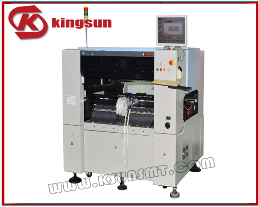
Product name: YV100XG YAMAHAmulti-functional chip mounter Product number: YV100XG Products in detail YAMAHA multi-function chip mounter YAMAHAYV100XG High speed and high precisionmulti-function modular placement machine 0.18 seconds/CHIP ultra-high-s
Used SMT Equipment | SMT Equipment
Product name: YV100XG YAMAHA multi-functional chip mounter Product number: YV100XG Products in detail YAMAHA multi-function chip mounter YAMAHA YV100XG High speed and high precision multi-function modular placement machine 0.18 seconds/CHIP ul
Industry News | 2003-02-07 08:34:04.0
Featuring Individual Instructors who, for Approximately 90 Minutes Each, will Speak on a Timely and Specific Topic
Industry News | 2015-07-06 10:34:12.0
The SMTA announces a new feature area that will debut during the SMTA International Electronics Exhibition: the “SMTA - NPL Solder Paste and Solder Joint Automatic Inspection Experience.” This special feature will take place during both days of the SMTA International Exhibition at the Donald Stephens Convention Center in Rosemont, Illinois on September 29 - 30, 2015.
Parts & Supplies | Assembly Accessories
Product name: YV100XG YAMAHAmulti-functional chip mounter Product number: YV100XG Products in detail YAMAHA multi-function chip mounter YAMAHAYV100XG High speed and high precisionmulti-function modular placement machine 0.18 seconds/CHIP ul
Technical Library | 2023-05-02 19:06:43.0
As 0402 has become a common package for printed circuit board (PCB) assembly, research and development on mounting 0201 components is emerging as an important topic in the field of surface mount technology for PWB miniaturization. In this study, a test vehicle for 0201 packages was designed to investigate board design and assembly issues. Design of Experiment (DOE) was utilized, using the test vehicle, to explore the influence of key parameters in pad design, printing, pick-andplace, and reflow on the assembly process. These key parameters include printing parameters, mounting height or placement pressure, reflow ramping rate, soak time and peak temperature. The pad designs consist of rectangular pad shape, round pad shape and home-based pad shape. For each pad design, several different aperture openings on the stencil were included. The performance parameters from this experiment include solder paste height, solder paste volume and the number of post-reflow defects. By analyzing the DOE results, optimized pad designs and assembly process parameters were determined.
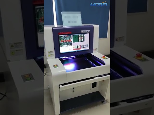
ML-A410 SMT Automated Optical Inspection Machine Feature ▶Economical and practical AOI. ▶High precision detection platform design. ▶Fast programming debugging integration. ▶Automatic recognize the Tip and Bottom side. ▶Professional SPC system.
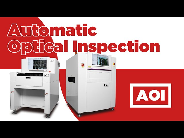
I.C.T Provide SMT Production Line solutions with Automated Optical Inspection (AOI) AOI is short for Automated Optical Inspection, which is widely used in the electronics industry to check the appearance of PCBA assembly at the back end of the cir
Career Center | Rochester, New York USA | Engineering
I have done my undergraduate studies in Mechanical Engineering. I am pursuing my Master's Program in Electronics Packaging. I am currently working as a Research Assistant for RIT-CEMA (Center for Electronics Manufacturing and Assembly). My research
Career Center | , | Engineering,Production
Project Management, SMT Process Engineering
| https://www.smtfactory.com/RS-1R-JUKI-Smt-High-Speed-Pick-And-Place-Machine-pd49094264.html
. Even faster assembly of smallest chips (0201 metric) up to large components of 50 x 150 mm or 74 mm edge length for square components
| https://ipcapexexpo.org/education/call-for-technical-paper-form
2.5-D/3-D Component Packaging BGA Packaging Connectors Design for Excellence (DFX) Design for Manufacturability (DFM) Design for Test (DFT) Die attach Embedded Passive and Active Devices Flexible Circuits Flip Chip/0201 Metric Package on Package Printed Electronics RFID Circuitry Re-balling Components Semiconductor Wire Bonding Other


winsouce.jpg)