Electronics Forum | Mon Aug 28 17:54:59 EDT 2000 | Steve Thomas
We're trying out 0603 packages on some 0805 footprints (at this stage only on some test boards) since our vendor tells us the 0805's are going to be getting harder to get, and more expensive to pay for. I understand the IPC footprint for the two is
Electronics Forum | Tue Nov 12 17:11:32 EST 2013 | mondalaci
Hi Folks, I'm working on a LED display that is composed of multiple layers. What is interesting for the point of this discussion is the PCB layer and the light deflector layer on top of it. Please take a look at the related pictures at http://plus
Industry News | 2017-05-11 17:06:16.0
Library Expert Lite automatically builds footprints and 3D STEP models for tens of millions of parts, for free.
Industry News | 2010-12-10 12:27:00.0
Ironwood Electronics recently introduced a new spring pin socket addressing precise resistance measurement need for testing power management devices - SSK-QFN-7000.
Parts & Supplies | Pick and Place/Feeders
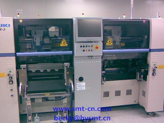
Starting in May 2008, JUKI Corporation (President Kazuyuki Nakamura; listed on First Section of the Tokyo Stock Exchange) is beginning worldwide sales of its High-speed Modular Mounter FX-3. The FX3 is an industrial robot for mounting electronic comp
Parts & Supplies | Pick and Place/Feeders
N310P917M PHOTO SENSOR SENSOR(原装全新) 5 A N310P916A OPTICAL FIBER CABLE,PLASTIC SENSOR(原装全新) 1 A N310E32T16P OPTICAL FIBER CABLE,PLASTIC SENSOR(原装全新) 1 A N1P61018NA OPTICAL INPUT OUTPUT UNIT 8
Technical Library | 2024-07-24 01:04:35.0
Quad Flat No Leads (QFN) package designs receive more and more attention in electronic industry recently. This package offers a number of benefits including (1) small size, such as a near die size footprint, thin profile, and light weight; (2) easy PCB trace routing due to the use of perimeter I/O pads; (3) reduced lead inductance; and (4) good thermal and electrical performance due to the adoption of exposed copper die-pad technology. These features make the QFN an ideal choice for many new applications where size, weight, electrical, and thermal properties are important. However, adoption of QFN often runs into voiding issue at SMT assembly. Upon reflow, outgassing of solder paste flux at the large thermal pad has difficulty escaping and inevitably results in voiding. It is well known that the presence of voids will affect the mechanical properties of joints and deteriorate the strength, ductility, creep, and fatigue life. In addition, voids could also produce spot overheating, lessening the reliability of the joints.
Events Calendar | Mon Jun 10 00:00:00 EDT 2024 - Mon Jun 10 00:00:00 EDT 2024 | Carlsbad, California USA
San Diego Chapter In-Person Event: IPC J-STD-001 Compliant Solder Pattern Calculations for DFA
| https://unisoft-cim.com/crosschecking-pcb-component-footprint-and-bom-footprint.html
of the 0603 shape components and 59 mils for the other 0603 component. Additional methods: IMPORT THE CAD OR GERBER FILE AND BOM AND CHECK THE FOOTPRINT DIMENSIONS: For aiding inspection in checking the component footprint on the PCB assembly ( PCBA
| https://www.eptac.com/faqs/ask-helena-leo/ask/smt-components-during-reflow-float-off-pads
SMT Components During Reflow Float Off Pads - EPTAC - Train. Work Smarter. Succeed Looking for solder training standards, manuals, kits, and more


