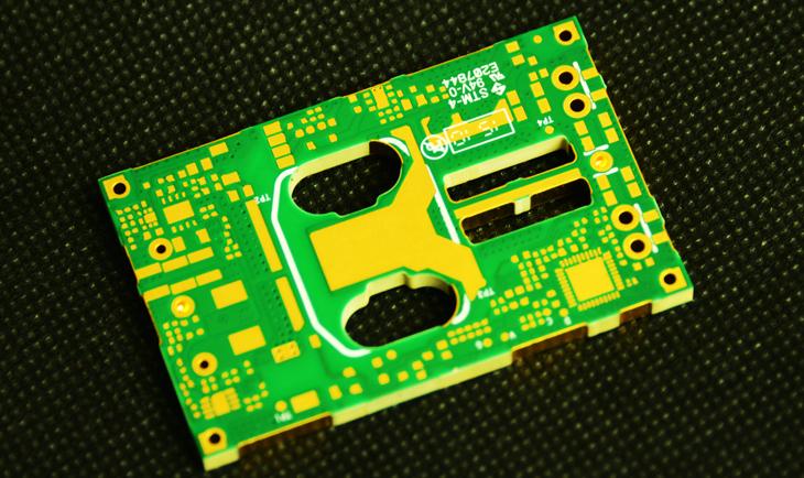
Project Description | Parameters 16 Layer Thickness: 3.8+/-0.03 mm Width/Space: 0.15mm/0.12 mm Surface Treatment: ENIG | Craft Material: SY ST115 Thermal Conductive:1.5W/m.k Back drilling, laser drilling | Application Electronic Power
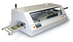
New Equipment | Wave Soldering
Cost effective, low to medium volume, automatic 8" single and dual wave soldering benchtop systems. Automatic wave solder system with self-contained fluxing, preheating and laminar (smooth) solder wave modules. Your Economic Solution for Easy St
Electronics Forum | Thu Jun 29 02:16:07 EDT 2006 | AR
We are experiencing some difficulties with reflow soldering a 1210-sized MOV with silver/palladium finish. The PCB finish is SAC. When inspecting the board after reflow it seems that nearly all solder is gone both from the pads and the component term
Electronics Forum | Tue Feb 04 22:28:16 EST 2003 | davef
You could reduce the paste by about 70%. Solder balling and tombstoning will be the issues to fight. The drivers to these don't change with the component size. Use the fine SMTnet Archives for background. Aperture Size and Thickness of Solder Pas
Industry News | 2014-03-25 09:35:06.0
Count On Tools Inc. (COT)announces the release of the new support plates for its line of ezLOAD Board Supports.
Industry News | 2003-08-27 10:43:02.0
This 41-page document is the complete source for printed circuit board and electronics assembly standards and publications for design, materials, manufacturing, assembly, quality and test.

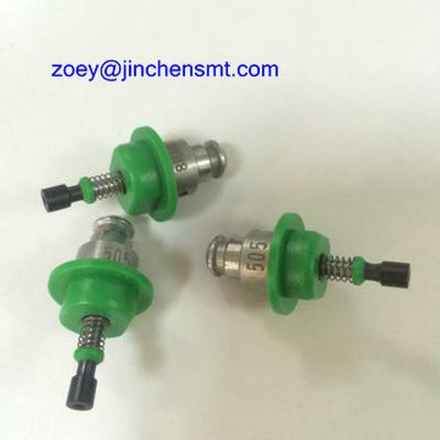
Parts & Supplies | Component Packaging
500 :0.5*0.3 501 :0.7*0.2 502 :0.7*0.4 503 :1.0*0.6 504 :1.5*1.0 505 :3.5*1.7 506 :5.0*3.2 507 :8.5*5.0 508 :9.3*8.0
Parts & Supplies | Component Packaging
500 :0.5*0.3 501 :0.7*0.2 502 :0.7*0.4 503 :1.0*0.6 504 :1.5*1.0 505 :3.5*1.7 506 :5.0*3.2 507 :8.5*5.0 508 :9.3*8.0


