Industry Directory | Consultant / Service Provider / Manufacturer
SemiPack Services is an Electronic Manufacturing Support Service to the semiconductor industry. We specialize in providing support services to high-mix low-volume (HMLV) customers
Industry Directory | Consultant / Service Provider / Manufacturer
PFC Flexible Circuits Limited designs, manufactures, and assembles flexible circuits; single-sided, double-sided, multilayer and rigid flex. We are ISO 9001 and 13485 approved.

New Equipment | Rework & Repair Equipment
BGA Rework Stations from the BGA Experts with over 25 years rework process experience and customer support! For high volume BGA Rework on even the largest computer and networking boards! The model SV560A has a high resolution optical system for pla
New Equipment | Solder Paste Stencils
Eliminate hours of solder mask damage repair time for bga sites while improving rework yield. Are you frustrated by the time it takes to repair mask damage underneath the BGA during the rework process? Are you squeezed for space on the PCB in an
Electronics Forum | Mon Oct 13 13:49:29 EDT 2003 | mrmaint
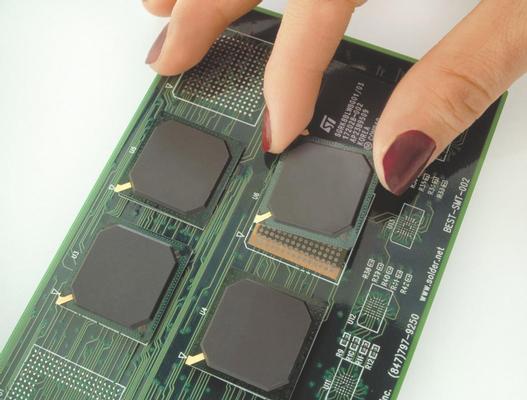
Does anyone know of a standard stencil thickness for BGA'S. We currently use 4 to 5 mil stencils depending on component mix. Is an aperature reduction required for BGA'S. If so what percentage. Any help would be greatly appreciated. Thanks MRMAINT
Electronics Forum | Thu Sep 12 01:49:28 EDT 2002 | ck
Hi all, Any stencil opening recommendation for 20mils pitch mirco BGA. Currently, using 12mils round opening, 5 mils thickness. Seen to have weak joints as it crack after Ict testing. thks
Used SMT Equipment | Pick and Place/Feeders
Tact time: 0.20sec/chip with line array camera Simultaneous pick with 8 heads 0.45 sec/SO with line array camera Simultaneous pick with 4 heads 1.4 sec/QFP with line array camera Sequential pick with 4 heads 3.7 sec/QFP with area CCD camera In fin
Used SMT Equipment | Pick and Place/Feeders
Tact time: 0.20sec/chip with line array camera Simultaneous pick with 8 heads 0.45 sec/SO with line array camera Simultaneous pick with 4 heads 1.4 sec/QFP with line array camera Sequential pick with 4 heads 3.7 sec/QFP with area CCD camera In fin
Industry News | 2003-07-02 08:54:26.0
A novel unreinforced, thermally conductive, pressure sensitive adhesive tape delivers very high bond strength to low-energy surfaces.
Industry News | 2010-02-17 18:45:59.0
The SMTA International Technical Committee invites you to submit an abstract for the 2010 conference. Short course descriptions are also being solicited.
Parts & Supplies | Repair/Rework
The RocHard 1 MilProbe is a 0.3" long Micro-tip in a 4 3/8" long hex shape stainless steel handle. The Micro-tip is tapered to a one mil diameter tip for TAB, BGA, and other ultra fine pitch rework. The tip is either straight (SH-341) or 50? angled a

Parts & Supplies | Chipshooters / Chip Mounters
SMT Nozzle for QP/QP132/QP242/QP341 FUJI QP242 INDEX SMT NOZZLE Part Number (OEM) Description ABHPN - 8510 ABHPN - 8520 ABHPN - 8530 ABHDN - 8560 ABHDN - 8570 ABHPN - 8590 QP-S-12 -ø 0.7 QP-S-12 NZ. ø 1.0 QP-S-12 NZ. ø 1.3 / 1.0 QP-M-38
Technical Library | 2023-07-25 16:42:54.0
Printing solder paste for very small components like .3mm pitch CSP's and 01005 Chip Components is a challenge for the printing process when other larger components like RF shields, SMT Connectors, and large chip or resistor components are also present on the PCB. The smaller components require a stencil thickness typically of 3 mils (75u) to keep the Area Ratio greater than .55 for good paste transfer efficiency. The larger components require either more solder paste height or volume, thus a stencil thickness in the range of 4 to 5 mils (100 to 125u). This paper will explore two stencil solutions to solve this dilemma. The first is a "Two Print Stencil" option where the small component apertures are printed with a thin stencil and the larger components with a thicker stencil with relief pockets for the first print. Successful prints with Keep-Outs as small as 15 mils (400u) will be demonstrated. The second solution is a stencil technology that will provide good paste transfer efficiency for Area Ratio's below .5. In this case a thicker stencil can be utilized to print all components. Paste transfer results for several different stencil types including Laser-Cut Fine Grain stainless steel, Laser-Cut stainless steel with and w/o PTFE Teflon coating, AMTX E-FAB with and w/o PTFE coating for Area Ratios ranging from .4 up to .69.
Technical Library | 2023-07-25 16:25:56.0
This paper address two significant applications of stencils in advance packaging field: 1. Ultra-Thin stencils for miniature component (0201m) assembly; 2. Deep Cavity stencils for embedded (open cavity) packaging. As the world of electronics continues to evolve with focus on smaller, lighter, faster, and feature-enhanced high- performing electronic products, so are the requirement for complex stencils to assemble such components. These stencil thicknesses start from less than 25um with apertures as small as 60um (or less). Step stencils are used when varying stencil thicknesses are required to print into cavities or on elevated surfaces or to provide relief for certain features on a board. In the early days of SMT assembly, step stencils were used to reduce the stencil thickness for 25 mil pitch leaded device apertures. Thick metal stencils that have both relief-etch pockets and reservoir step pockets are very useful for paste reservoir printing. Electroform Step-Up Stencils for ceramic BGA's and RF Shields are a good solution to achieve additional solder paste height on the pads of these components as well as providing exceptional paste transfer for smaller components like uBGAs and 0201s. As the components are getting smaller, for example 0201m, or as the available real estate for component placement on a board is getting smaller – finer is the aperture size and the pitch on the stencils. Aggressive distances from step wall to aperture are also required. Ultra-thin stencils with thicknesses in the order of 15um-40um with steps of 15um are used to obtain desired print volumes. Stencils with thickness to this order can be potential tools even to print for RDLs in the package.
High Performance Customized Reflow Oven for Radiator ❙ Introduce of Reflow Oven ETA provide high reliability special reflow oven, SMD reflow soldering oven, radiator reflow oven, hot air reflow oven, for radiator production line. Spec
SMT Reflow Ovens for PCB Soldering ❙ Introduce of Reflow Soldering Oven High quality SMT reflow ovens, PCB soldering oven machine, lead-free reflow oven, for PCB soldering. ETA SMT machines manufacturers offers from 6-12 zones good price ref
Training Courses | ONLINE | | ESD Control Training Courses
Browse training and certification programs for electrostatic discharge (ESD) control in electronics assembly.
Training Courses | | | Other Courses
Other courses related to electronics manufacturing and assembly
Career Center | San Jose, California USA | Engineering,Research and Development
www.srqconsultants.com : for job reqs Type of job background: Design for Test (DFT), with ATE Test development experience, and an IC design generalist. Job Summary Must have +5 years industry experience combination in IC Design and ATE test. Som
Career Center | Garland, Texas USA | Sales/Marketing
Electronics Manufacturing Company is looking for FT/PT full commission sales personnel, 25% and up commission base on value of orders ( not the bottom line). Experience on handling own sales accounts. Extra income for referrals, if you have business
Career Center | , | Engineering,Production
Project Management, SMT Process Engineering
Career Center | Erode, Tamilnadu India | Engineering
Professional Summary 3+ years of experience in the PCB CAM engineering Exposure to FRONTLINE GENESIS 2000 Having exposure in UCAM Exposure to Create, Array & Panelize it for manufacturability Experienced in Creating impedance cou
| https://www.eptac.com/faqs/ask-helena-leo/page/5
Ask Helena & Leo (5) Looking for solder training standards, manuals, kits, and more? Visit soldertraining.com Training Training Materials Locations Resources Ask Helena
Heller Industries Inc. | https://hellerindustries.com/wp-content/uploads/2018/07/last-will-of-bga-void.pdf
“The Effects of Solder Joint Voiding on Plastic Ball Grid Array Reliability” [5] Investigation Specifics: 225 I/O Plastic BGA, daisy chained, 0.762mm (30 mil
winsouce.jpg)


