New Equipment | Test Equipment
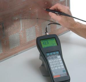
The hand-held PHASCOPE® PMP10 is ideally suited for quality control in the electroplating and printed circuit board (PCB) industries. Because the instrument employs the phase-sensitive eddy current method (ISO 21 968), it allows the measurement of me
Electronics Forum | Mon May 13 23:44:26 EDT 2019 | dami0629
if use tray cannot solve the problem, you can change from the design 1)Reduce the effect of temperature on PCB 2) PCB USE HIGH TG 3) BOARD THICKNESS TOO THIN 4) MODIFY THE BOARD SIZE 5) Reduce the V-CUT depth.
Electronics Forum | Mon Jul 01 09:33:08 EDT 2019 | dbuschel
if you can't change the PCB materials or design at this point, you might be able to reduce it somewhat through the use of fixtures or edge stiffeners. Unless it is a particularly thick board, I don't think the reflow profile would be the issue. The t
Industry News | 2011-01-12 17:48:44.0
GPD Global will highlight its Positive Cavity Displacement (PCD) Dispensing in Booth #6111 at the upcoming Automation and Technology West Expo (ATX), scheduled to take place February 8-10, 2011 at the Anaheim Convention Center in Anaheim, CA.
Industry News | 2023-04-11 09:52:04.0
MIRTEC will premier its complete line of 3D AOI and SPI Inspection Systems at SMTconnect, scheduled to take place May 9-11, 2023 in Nuremberg, Germany. The company will showcase a total of five (5) Inspection Systems specifically designed to address the full spectrum of inspection requirements associated with the electronics manufacturing industry in Hall 4A, Stand 128.

Parts & Supplies | Pick and Place/Feeders
Many companies first applied SMT second-hand placement machines, and the selected placement machines were relatively stable, with low failure rate, easy maintenance, and important maintenance costs. Therefore, there are still many concerns about buyi
Parts & Supplies | Pick and Place/Feeders
Many companies first applied SMT second-hand placement machines, and the selected placement machines were relatively stable, with low failure rate, easy maintenance, and important maintenance costs. Therefore, there are still many concerns about buyi
Technical Library | 2018-03-21 22:44:30.0
Solder paste printing is the first step in the surface mount manufacturing process for PCBA assembly. When the solder paste printing process is uncontrolled, defects can be produced, which may not become apparent until the PCBA is downstream. (...)This paper will discuss how Lean Six Sigma techniques were used to optimize the solder paste printing process. It will highlight how a cross-functional team used the structured Define, Measure, Analyze, Improve and Control (DMAIC) methodology to identify and control the critical inputs. The advantage of the Lean Six Sigma methodology is that it guides the team through the rigorous structured process so that all possible inputs are considered and the critical ones can be identified.
Technical Library | 2020-08-27 01:22:45.0
Initially adopted internal specifications for acceptance of printed circuit boards (PCBs) used for wire bonding was that there were no nodules or scratches allowed on the wirebond pads when inspected under 20X magnification. The nodules and scratches were not defined by measurable dimensions and were considered to be unacceptable if there was any sign of a visual blemish on wire-bondable features. Analysis of the yield at a PCB manufacturer monitored monthly for over two years indicated that the target yield could not be achieved, and the main reasons for yield loss were due to nodules and scratches on the wirebonding pads. The PCB manufacturer attempted to eliminate nodules and scratches. First, a light-scrubbing step was added after electroless copper plating to remove any co-deposited fine particles that acted as a seed for nodules at the time of copper plating. Then, the electrolytic copper plating tank was emptied, fully cleaned, and filtered to eliminate the possibility of co-deposited particles in the electroplating process. Both actions greatly reduced the density of the nodules but did not fully eliminate them. Even though there was only one nodule on any wire-bonding pad, the board was still considered a reject. To reduce scratches on wirebonding pads, the PCB manufacturer utilized foam trays after routing the boards so that they did not make direct contact with other boards. This action significantly reduced the scratches on wire-bonding pads, even though some isolated scratches still appeared from time to time, which caused the boards to be rejected. Even with these significant improvements, the target yield remained unachievable. Another approach was then taken to consider if wire bonding could be successfully performed over nodules and scratches and if there was a dimensional threshold where wire bonding could be successful. A gold ball bonding process called either stand-off-stitch bonding (SSB) or ball-stitch-on-ball bonding (BSOB) was used to determine the effects of nodules and scratches on wire bonds. The dimension of nodules, including height, and the size of scratches, including width, were measured before wire bonding. Wire bonding was then performed directly on various sizes of nodules and scratches on the bonding pad, and the evaluation of wire bonds was conducted using wire pull tests before and after reliability testing. Based on the results of the wire-bonding evaluation, the internal specification for nodules and scratches for wirebondable PCBs was modified to allow nodules and scratches with a certain height and a width limitation compared to initially adopted internal specifications of no nodules and no scratches. Such an approach resulted in improved yield at the PCB manufacturer.
https://www.ascen.ltd/Products/Automatic_SMT_equipment/PCB_conveyor/100.html PCB linking conveyor and PCB belt conveyor mainly used to connect different type PCB board handing equipment effectively for the SMT production line. ASCEN technology is ava
https://www.ascen.ltd/Products/Automatic_SMT_equipment/PCB_conveyor/100.html PCB linking conveyor and PCB belt conveyor mainly used to connect different type PCB board handing equipment effectively for the SMT production line. ASCEN technology is ava
---> SMT Express, Volume 3, Issue No. 6 - from SMTnet.com Volume 3, Issue No. 6 Friday, June 15, 2001 Featured Article Return to Front Page PCB Assembly Techniques by Harvey Twyman , University of Kent at Canterbury "I'm sure you
Imagineering, Inc. | https://www.pcbnet.com/blog/hdi-pcb-advantages-and-applications/
HDI PCB: Advantages and Applications | Imagineering, Inc. Skip to main content Resources Support Contact Us FAQs Live Chat My Account 847-806-0003 Menu PCB Capabilities Fabrication Technology Roadmap Materials Available HDI Tolerances Certifications
PCB Libraries, Inc. | https://www.pcblibraries.com/forum/RSS_3d-model-using-pcb-library-expert-pro-2016_topic2400.xml
(Mechanical Layer 13 assigned for 3D Model in Altium). Do I need to import 3D model? If I don't import 3D model, PCB Library Expert Pro 2016 will generate based on the information provided?Regards,Rafiq

Products, services, training & consulting for the assembly, rework & repair of electronic assemblies. BGA process experts. Manufacturers Rep, Distributor & Service Provider for Seamark/Zhuomao and Shuttle Star BGA Rework Stations.
Training Provider / Manufacturer's Representative / Equipment Dealer / Broker / Auctions / Consultant / Service Provider
1750 Mitchell Ave.
Oroville, CA USA
Phone: (888) 406-2830


