Industry Directory | Manufacturer
The exclusive supplier of SIPAD Solid Solder Deposit in North America and the only SIPAD Solid Solder Deposit (SSD) coating service bureau in the world.
Industry Directory | Consultant / Service Provider / Manufacturer
A Contract Manufacturing company specializing in Printed Circuit Board Assembly, Quick Turn Prototype Services, and Direct Fulfillment.
New Equipment | Rework & Repair Equipment
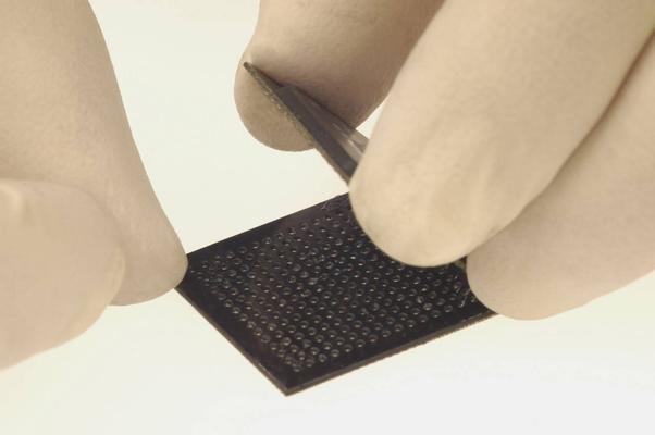
The BEST EZReball™ process is the answer to your reballing problems. This BGA reballing process simplifies the process while eliminating the clean up of all those paper remnants, allowing for better yields and faster reballing times. The simplicity o
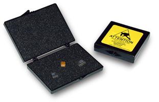
PillowStat ESD, CCI's new concept in component packaging includes (2) 1/4" conductive foam 'pillow pads' inside a static shielding injection molded plastic box. This package is designed to safely package one or more ESd sensitive devices without cust
Electronics Forum | Tue Jun 21 11:46:04 EDT 2005 | kenscj
Hi dave, Thanks for the comment. I have another issue. The board already pass Test and Burn-In processes, but after 2 months the BGA contact is found open (no contact on certain balls). How can that happen? Is it during build, the solder ball alrea
Electronics Forum | Tue Jun 06 11:57:12 EDT 2006 | Chunks
IPC 610 says acceptable Class 1 (Class 2, 3 indicator) if they are entrapped/encpsulated balls within 0.13mm of lands or pads. or exceed 0.13mm in diameter. Defect Class 1,2,3: Solder ball violates min electrical clearance. Solder balls not entrap
Used SMT Equipment | Pick and Place/Feeders
Highlights of the SIPLACE CA: With the four SIPLACE SpeedStar heads for high-precision placements you can process up to 126,000 SMT components, 46,000 flip-chips, or 30,000 die-attach components per hour Component supplied from changeov
Industry News | 2011-03-31 11:54:23.0
Over the past few years, pad cratering has become a vexing problem in lead-free assemblies, largely attributed to problems with the resin used to make a printed board. To help industry eliminate the defect and, at the same time, cut costs, IPC — Association Connecting Electronics Industries® has released IPC-9708, Test Methods for Characterization of PCB Pad Cratering.
Industry News | 2013-01-30 17:54:43.0
Design, assembly, inspection and repair personnel have a new tool to help improve reliability of ball grid arrays (BGAs) and fine-pitch ball grid arrays (FBGAs) in high density applications, thanks to the newly released C revision of IPC-7095, Design and Assembly Process Implementation for BGAs.
Technical Library | 2022-10-31 17:09:04.0
The global transition to lead-free (Pb-free) electronics has led component and equipment manufacturers to transform their tin–lead (SnPb) processes to Pb-free. At the same time, Pb-free legislation has granted exemptions for some products whose applications require high long-term reliability. However, due to a reduction in the availability of SnPb components, compatibility concerns can arise if Pb-free components have to be utilized in a SnPb assembly. This compatibility situation of attaching a Pb-free component in a SnPb assembly is generally termed "backward compatibility." This paper presents the results of microstructural analysis of mixed solder joints which are formed by attaching Pb-free solder balls (SnAgCu) of a ball-grid-array component using SnPb paste. The experiment evaluates the Pb phase coarsening in bulk solder microstructure and the study of intermetallic compounds formed at the interface between the solder and the copper pad.
Technical Library | 2020-08-27 01:22:45.0
Initially adopted internal specifications for acceptance of printed circuit boards (PCBs) used for wire bonding was that there were no nodules or scratches allowed on the wirebond pads when inspected under 20X magnification. The nodules and scratches were not defined by measurable dimensions and were considered to be unacceptable if there was any sign of a visual blemish on wire-bondable features. Analysis of the yield at a PCB manufacturer monitored monthly for over two years indicated that the target yield could not be achieved, and the main reasons for yield loss were due to nodules and scratches on the wirebonding pads. The PCB manufacturer attempted to eliminate nodules and scratches. First, a light-scrubbing step was added after electroless copper plating to remove any co-deposited fine particles that acted as a seed for nodules at the time of copper plating. Then, the electrolytic copper plating tank was emptied, fully cleaned, and filtered to eliminate the possibility of co-deposited particles in the electroplating process. Both actions greatly reduced the density of the nodules but did not fully eliminate them. Even though there was only one nodule on any wire-bonding pad, the board was still considered a reject. To reduce scratches on wirebonding pads, the PCB manufacturer utilized foam trays after routing the boards so that they did not make direct contact with other boards. This action significantly reduced the scratches on wire-bonding pads, even though some isolated scratches still appeared from time to time, which caused the boards to be rejected. Even with these significant improvements, the target yield remained unachievable. Another approach was then taken to consider if wire bonding could be successfully performed over nodules and scratches and if there was a dimensional threshold where wire bonding could be successful. A gold ball bonding process called either stand-off-stitch bonding (SSB) or ball-stitch-on-ball bonding (BSOB) was used to determine the effects of nodules and scratches on wire bonds. The dimension of nodules, including height, and the size of scratches, including width, were measured before wire bonding. Wire bonding was then performed directly on various sizes of nodules and scratches on the bonding pad, and the evaluation of wire bonds was conducted using wire pull tests before and after reliability testing. Based on the results of the wire-bonding evaluation, the internal specification for nodules and scratches for wirebondable PCBs was modified to allow nodules and scratches with a certain height and a width limitation compared to initially adopted internal specifications of no nodules and no scratches. Such an approach resulted in improved yield at the PCB manufacturer.

LED panel is a kind of flat panel display which is composed of small LED modules. It is the largest and most widely used large-screen panel technology at present. It can be used not only indoors but also outdoors, waterproof, windproof and rain proo
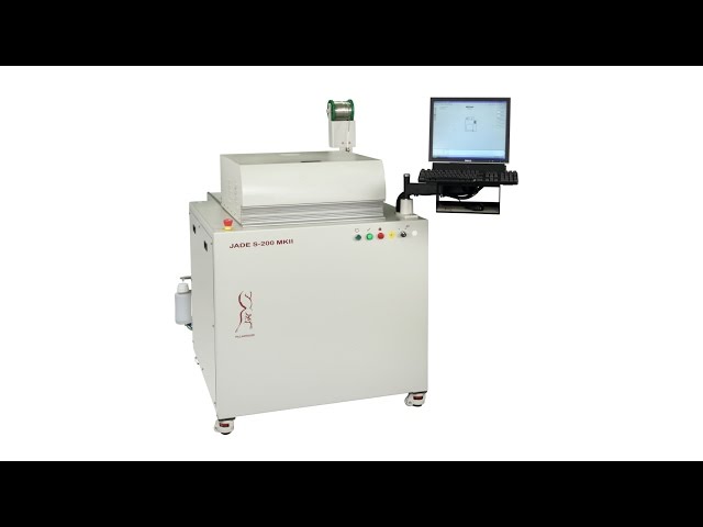
To see more about the Jade MKII Single Point Selective Soldering System visit Pillarhouse USA at: https://www.pillarhouse.co.uk/products/selective-soldering-handload/jade-mkii-handload Entry-level, single point selective soldering system Designed t
Events Calendar | Mon Apr 23 00:00:00 EDT 2018 - Thu Apr 26 00:00:00 EDT 2018 | Shanghai, China
SMTA China East Conference 2018
Career Center | South Plainfield, New Jersey USA | Engineering
Alpha, a business unit of Alent plc and the global leader in the development, manufacturing and sales of innovative specialty materials used in a wide range of industry segments, including electronics assembly, power electronics, die attach, LED ligh
Career Center | Brooklyn, New York USA | Engineering,Production
Mini-Circuits designs, manufactures and distributes integrated circuits, modules, and sub-systems for high performance radio frequency (RF) and microwave applications. With design, sales and manufacturing locations in over 30 countries, Mini-Ci
SMTnet Express, May 9, 2019, Subscribers: 31,902, Companies: 10,760, Users: 26,083 Cold Ball Pull Test Efficiency for the PCB Pad Cratering Validation with the Ultra Low Loss Dielectric Material Credits: iNEMI (International Electronics
SMT Express, Volume 2, Issue No. 3 - from SMTnet.com Volume 2, Issue No. 3 Thursday, March 16, 2000 Featured Article Return to Front Page Curtailing Voids in Fine Pitch Ball Grid Array Solder Joints by Gary Morrison and Kevin Lyne
ASYMTEK Products | Nordson Electronics Solutions | https://www.nordson.com/en/divisions/dage/test-types/first-bond-ball-pull-stud-bump-pull?con=t&page=7
. First bond ball pull utilises cold bump pull jaw technology to apply a vertical load (a pull test) to ball bonds and stud bumps. Ball shear tests can sometimes promote pad cratering due to the aggressive nature of the bonding process which can weaken the ball bonds
| https://www.smtfactory.com/What-is-the-LED-Display-SMT-Production-Process-id41946657.html
What is the LED Display SMT Production Process? - I.C.T SMT Machine English Bahasa indonesia Сербия Česky Dansk Deutsch Español Français Hrvatski Italiano magyar Nederlands Polski


