Industry Directory | Manufacturer
Buyers of Scrap Materials and Surplus Machinery, Equipment and Inventories Precious Metal Refining Warehouse Liquidation PCB & Electronic Scrap Recycling Purchasing of Used Surplus Semiconductor
Electronics Forum | Wed Jan 30 03:20:00 EST 2019 | bane016
We measure each first board before the oven after every chageover...Assembling one offset and measure component, after we clear plate...We have reason why do that...But we're wasting a lot of time.So I wanted to see how you do it. Thank you for answe
Electronics Forum | Sun Jun 21 18:06:45 EDT 1998 | Fred Dub
New developments in bulk feeding are making this process of feeding passive components more and more attractive to the PCB manufacturers, for whom the tape feeding for a long time was the solution. The rapid growth in the number of passive component

Used SMT Equipment | Circuit Board Assembly Products
Lowest stress, no dust, no sundries on the fringe of PCB, Especialy for separate the aluminium PCB. Description: The SM-3000 type depanning machines were designed to depanerlize prescored panelboards carefully without bending or tension stress, ev
Industry News | 2023-04-06 16:07:01.0
Novel Pulsiv OSMIUM technology delivers high power factor, consistently high efficiency up to 99.5%, in an ultra-compact system design. Pulsiv OSMIUM power electronics technology can be used to improve overall system efficiency, and optimize BOM cost.
Technical Library | 2020-08-13 00:59:03.0
The paper will discuss the integration of 3D printing and inkjet printing fabrication technologies for microwave and millimeter-wave applications. With the recent advancements in 3D and inkjet printing technology, achieving resolution down to 50 um, it is feasible to fabricate electronic components and antennas operating in the millimeter-wave regime. The nature of additive manufacturing allows designers to create custom components and devices for specialized applications and provides an excellent and inexpensive way of prototyping electronic designs. The combination of multiple printable materials enables the vertical integration of conductive, dielectric, and semi-conductive materials which are the fundamental components of passive and active circuit elements such as inductors, capacitors, diodes, and transistors. Also, the on-demand manner of printing can eliminate the use of subtractive fabrication processes, which are necessary for conventional microfabrication processes such as photolithography, and drastically reduce the cost and material waste of fabrication.
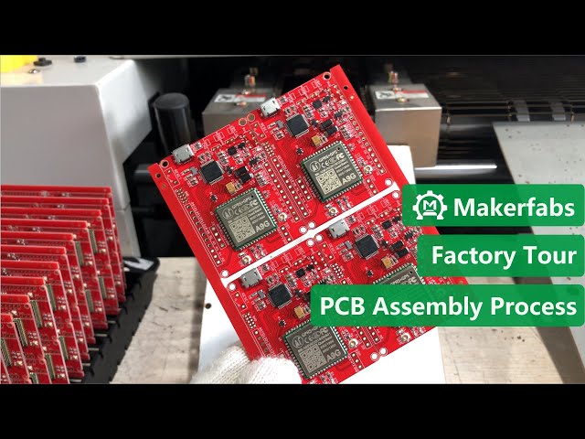
In the world of makers, people enjoy the fun of designing and developing hardware/ software, even final electronic products. They will not concentrate a lot on the cost and manufacturability. But it is quite different from lab to factory, when it com
Career Center | Farrukh Hussain, Pakistan | Engineering,Maintenance
PLC, SCADA, designing circuit or PCB layout, troubleshooting and maintenance, electrical and instrumentation, electronics design, software skill with programming.
Career Center | Karachi, Pakistan | Engineering,Maintenance
PLC, SCADA, designing circuit or PCB layout, troubleshooting and maintenance, electrical and instrumentation, electronics design, software skill with programming.


