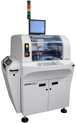
High Precision Dispensers - MAX Series (Non-Heated) Max Series is capable of a wide variety of dispense applications including MicroVolume, Solder Paste and Conductive Adhesive, Underfill, Surface Mount Adhesive, Dam and Fill, Encapsulations, LED En
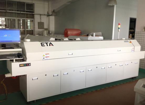
Full Hot Air Lead-Free Reflow Oven With PC Temp Control System (A800) Introduce: 1, Heating system adopts ETA patent heating technology 2, The use of imported large current solid state relay contact output, safe, reliable, equipped with a dedicated
Electronics Forum | Tue Nov 27 07:44:59 EST 2007 | davef
We do not paste when we glue. We glue components so they will stay inplace during wave soldering. In wave soldering there is ample solder to bridge the standoff between the component and the pad.
Electronics Forum | Tue Nov 27 07:51:21 EST 2007 | shy
is there any gap between the pad and terminal if we place the glue? Btw, my practice to print solder pate then punch glue then PNP component and finally reflow. Also we find drop/missing chip after wave eventhough we glue the component.
Used SMT Equipment | Turnkey Lines
Functional Pre-Owned Complete SMT Assembly Line - Still Operational (Subject to prior sell, I am listing this on other venues) Up for sale is a full turnkey SMT line and all of it's accessories, of which there are a lot, fe
Industry News | 2011-07-26 22:29:00.0
It’s well-known that residues on printed board assemblies can lead to serious reliability problems. To help the process engineering community deal with these difficulties, IPC has released the B revision of IPC-CH-65, Guidelines for Cleaning of Printed Boards & Assemblies.
Industry News | 2017-11-08 15:17:48.0
Nordson ASYMTEK will introduce a powerful array of new products, technologies, and solutions for conformal coating and automated fluid dispensing at Productronica 2017 in Hall A2, stand 345.
Technical Library | 2022-12-19 18:59:51.0
Material and Process Characterization studies can be used to quantify the harmful effects that might arise from solder flux and other process residues left on external surfaces after soldering. Residues present on an electronic assembly can cause unwanted electrochemical reactions leading to intermittent performance and total failure. Components with terminations that extend underneath the package can trap flux residue. These bottom terminated components are flush with the bottom of the device and can have small solderable terminations located along the perimeter sides of the package. The clearance between power and ground render high electrical forces, which can propagate electrochemical interactions when exposed to atmospheric moisture (harsh environments). The purpose of this research is to predict and understand the functional performance of residues present under single row QFN component packages. The objective of the research study is to develop and collect a set of guidelines for understanding the relationship between ionic contamination and electrical performance of a BTC component when exposed to atmospheric moisture and the trade-offs between electrical, ionic contamination levels, and cleanliness. Utilizing the knowledge gained from undertaking the testing of QFN components and associated DOE, the team will establish a reference Test Suite and Test Spec for cleanliness.
Technical Library | 2023-05-02 19:03:34.0
The demand for 0201 components in consumer products will increase sharply over the next few years due to the need for miniaturization. It is predicted that over 20 billion 0201 components will be used in more than one billion cell phones worldwide by the year 2003. Therefore, research and development on 0201 assembly is becoming a very hot topic. The first step to achieve a successful assembly process is to obtain a good PCB design for 0201 packages. This paper presents the data and criteria of PCB design for 0201 packages, including the pad design for 0201 components, and the minimum pad spacing or component clearance between 0201 components or between 0201 and other components. A systematic study on pad design and pad spacing was undertaken, using two test vehicles and three Design of Experiments (DOEs). In the first DOE, 2 out of 18 types of 0201 pad designs were selected based on process yield. The second DOE was focused on pad spacing, including 10mil, 8mil, 6mil and 4mil. The third experiment was final optimization, using two types of optimized pad designs with 10mil, 8mil and 6mil pad spacing. Through the above experiments, the design guideline for PCB layout for 0201 packages and the assembly process capability are identified.
Full Hot Air Lead-Free Reflow Oven With PC Temp Control System (A800) Introduce: 1, Heating system adopts ETA patent heating technology 2, The use of imported large current solid state relay contact output, safe, reliable, equipped with a dedicated
Main product: SMT Assembly Reflow Oven, SMT Hot Air Reflow Oven, Lead Free Reflow Oven, SMT Reflow Oven, SMT Mounting Machine, Elctronic Equipment, PCB Machine, reflow oven, SMT Assembly, SMT/SMD Equipment, PCB Printer, screen printing SMT assembly
GPD Global | https://www.gpd-global.com/co_website/pdf/lead-former/CF8-User-Guide-801-1-07.pdf
) and remove the component ejector blade (Item 1) from between the transport wheel pair (Item 4). b) Place a 1/8-inch bent hex "T" wrench (provided in the tool kit) in the hole located toward the end of the transport wheel shaft (Item 5) and pull firmly
PCB Libraries, Inc. | https://www.pcblibraries.com/Forum/overlay-clearance-to-include-solder-mask_topic2267.html
0.12 mm (5 mil) gap between the Legend and Pad. The typical solder mask swell today is 0.075 mm (3 mil) and many component mfr.'s are calling out 0.05 mm (2 mil


