New Equipment | Rework & Repair Equipment
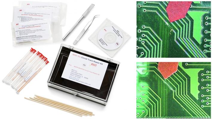
The BEST PCB circuit trace repair kit gives you the tools you need for fast modification and repair of PCB circuit traces. Our online PCB repair training videos, our master instructors along with these materials allows you to meet the original PCB qu
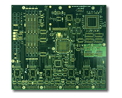
8 layers board Basic Material: FR-4 Board Ply (thickness): 1.80mm Measurement: 254mm x 304.8mm Conductor Width: 5mil (0.13mm) Conductor Spacing: 5mil (0.13mm) Surface Treatment: Immersion gold File Format: Gerber File (RS274X) Through Hole: 2
Electronics Forum | Tue Nov 09 05:14:49 EST 1999 | Wolfgang Busko
Hi all, our problem we face is the mismatch of conductor width on the delivered PCB and the nominal width given by CAD-data. With CAD we are improving pads and conductors to match the specific needs for soldering and the board houses counteract our i
Electronics Forum | Tue Nov 09 11:32:32 EST 1999 | Dave F
Wolfgang: "Our desire is to get what we design" ... Wanting to get what you ask for ... ummm sounds like a risky proposition!!! ;-) Two things: 1 Go to the Hadco site and get their "boiler-plate." Use it and some of the Earl Moon specs in the SMTn
Industry News | 2004-09-07 18:32:13.0
NORTHBROOK, Ill., September, 2004
Parts & Supplies | Pick and Place/Feeders
JUKI EA9500B0000 CLIP CV-70S www.fujintai.com JUKI EA9500B0100 CABLE BAND FUJINTAI TECHNOLOGY CO.,LTD JUKI EA9500B0200 CABLE BAND 150 www.fujintai.com JUKI EA9635B0000 SOCKET FUJINTAI TECHNOLOGY CO.,LTD JUKI ES000175000 8 STAINLESS TUBE N2 www.fu
Parts & Supplies | Assembly Accessories
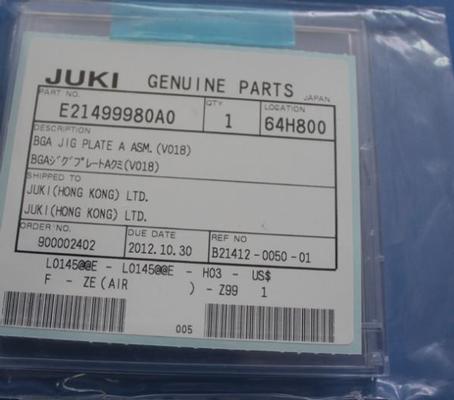
JUKI NGA JIP PLATE A ASM E21499980A0 We are Supply SMT Pick and Place Equipment spare parts(Smt nozzle, Smt Cylinder, Smt Valve, Smt Sensor, Smt Feeder, Smt CPU Board, Smt Laser, Smt driver, Smt ejector……) for Yamaha, JUKI, FUJI ,Panasonic, Samsun
Technical Library | 2021-05-06 13:45:49.0
The high-sensitive micro eddy-current testing (ECT) probe composed of planar meander coil as an exciter and spin-valve giant magneto-resistance (SV-GMR) sensor as a magnetic sensor for bare printed circuit board (PCB) inspection is proposed in this paper. The high-sensitive micro ECT probe detects the magnetic field distribution on the bare PCB and the image processing technique analyzes output signal achieved from the ECT probe to exhibit and to identify the defects occurred on the PCB conductor. The inspection results of the bare PCB model show that the proposed ECT probe with the image processing technique can be applied to bare PCB inspection. Furthermore, the signal variations are investigated to prove the possibility of applying the proposed ECT probe to inspect the high-density PCB that PCB conductor width and gap are less than 100 μm.
Technical Library | 2020-03-26 14:55:29.0
This paper introduces line confocal technology that was recently developed to characterize 3D features of various surface and material types at sub-micron resolution. It enables automatic microtopographic 3D imaging of challenging objects that are difficult or impossible to scan with traditional methods, such as machine vision or laser triangulation.Examples of well-suited applications for line confocal technology include glossy, mirror-like, transparent and multi-layered surfaces made of metals (connector pins, conductor traces, solder bumps etc.), polymers (adhesives, enclosures, coatings, etc.), ceramics (components, substrates, etc.) and glass (display panels, etc.). Line confocal sensors operate at high speed and can be used to scan fast-moving surfaces in real-time as well as stationary product samples in the laboratory. The operational principle of the line confocal method and its strengths and limitations are discussed.Three metrology applications for the technology in electronics product manufacturing are examined: 1. 3D imaging of etched PCBs for micro-etched copper surface roughness and cross-sectional profile and width of etched traces/pads. 2. Thickness, width and surface roughness measurement of conductive ink features and substrates in printed electronics applications. 3. 3D imaging of adhesive dots and lines for shape, dimensions and volume in PCB and product assembly applications.

This video describes the IPC A-600 training and certification program. The IPC A-600 specification is a set of acceptability specifications for printed circuit boards. These standards determine the acceptance and reject criteria for printed wiring bo
This video describes the IPC A-600 training and certification program. The IPC A-600 specification is a set of acceptability specifications for printed circuit boards. These standards determine the acceptance and reject criteria for printed wiring bo
Training Courses | | | IPC-600 Specialist (CIS)
The Certified IPC-600 Specialist (CIS) training targets quality assurance and acceptance of bare printed circuit boards.
Training Courses | | | IPC-600 Specialist (CIS)
The Certified IPC-600 Specialist (CIS) training targets quality assurance and acceptance of bare printed circuit boards.
ASYMTEK Products | Nordson Electronics Solutions | https://www.nordson.com/en/applications/mixing?con=t&page=29
: Adhesive Mixing Applications Summit Lamination Applicators Data Sheet Adhesive Dispensing Systems Deliver superior control of fiber size, density and pattern width in backsheet lamination and core
GPD Global | https://www.gpd-global.com/co_website/pdf/doc/Dispense-System-Service-Guide-22290008G.pdf
deteriorated belts. Refer to REMOVE / REPLACE Conveyor Belt (pg 5.86). • Inspect belts for signs of excessive wear. • Inspect belt seams for signs of deterioration or failure. X X Conveyor width adjust unit If a conveyor is present, inspect for loose or worn


