Industry Directory | Manufacturer's Representative
Manufacturer's representative located in Florida.
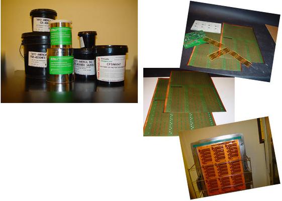
New Equipment | Solder Materials
Liquid Photoimageable Solder Application Since the introduction of Liquid Photoimageable Solder Masks (LPSIM) in the late 1980's, SolderMask, Inc. has continued to be the premier service-bureau applying it to PCB's. SolderMask, Inc. was the first
Electronics Forum | Thu Apr 22 10:57:20 EDT 1999 | Jack Coia
On various PCB's after building processes,such as reflow, flowsolder and wash. The soldermask on the PCB's have become discoloured, like a 'marble' effect all along the solder side of the board, it is lighter in contrast than normal, although when ot
Electronics Forum | Thu Apr 22 18:07:38 EDT 1999 | Tom B.
| On various PCB's after building processes,such as reflow, flowsolder and wash. The soldermask on the PCB's have become discoloured, like a 'marble' effect all along the solder side of the board, it is lighter in contrast than normal, although when
Industry News | 2019-11-05 22:07:01.0
Tenting a via refers to covering via with soldermask to enclose or skin over the opening. A via is a hole drilled into the PCB that allows multiple layers on the PCB to be connected to each other. A non tented via is just a via that is not covered with the soldermask layer. Leaving these vias exposed or covered has pros and cons depending on the your design and manufacturing requirements.
Industry News | 2018-10-18 11:08:57.0
What are PCB Thickness Options?
Technical Library | 2019-09-19 00:28:48.0
The symbiotic relationship between solder masks and selective finishes is not new. The soldermask application is one of the key considerations to ensure a successful application of a selective finish. The selective finish is the final chemical step of the PCB manufacturing process, this is when the panels are at their most valuable and are unfortunately not re-workable. Imperfections are not tolerated, even if they are wholly cosmetic. Quality issues often manifest themselves in the form of a 'ping pong' conversation between the fabricators, the soldermask suppliers and the selective finish suppliers. Without tangible evidence these discussions are difficult to resolve and the selective finish process is usually regarded as responsible. This paper will focus on the chemical characteristics and use them to predict or identify potential issues before they occur rather than specifically name 'critical' soldermasks. It is also the intention of this paper to address the potential of a soldermask to react to common yield hiking practices like UV bumping and oven curing. It is hoped that this awareness will help fabricators to ensure maximum yields by asking the right questions. 'Critical’ soldermasks impact all selective finishes. In this paper, practical experience using immersion tin will be used to highlight the relationship between 'critical' soldermasks and some of the issues seen in the field. The paper will include a novel approach to identify re-deposited volatiles after the reflow.


.png)

