New Equipment | Test Equipment
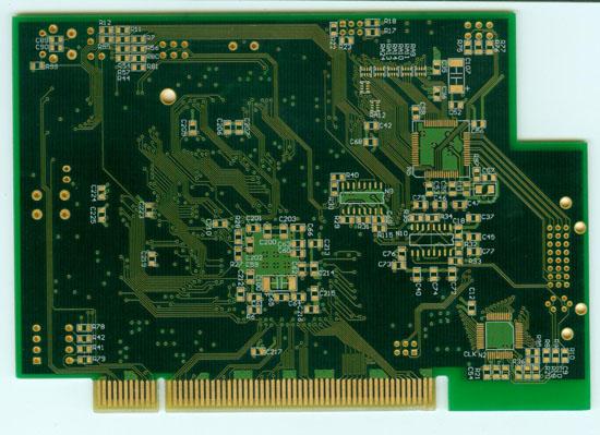
Printed Circuit Boards(PCBs) are used to electrically connect electronic components using conductive pathways, traces, etched from copper sheets laminated onto a non-conductive substrate. Our manufacturing processes utilise the latest techniques an
New Equipment | Solder Materials
AuSn solder electroplating is a key technology developed by Micralyne to lower your production costs and give you a better MEMS product. This state-of-the-art, patented process for electroplating AuSn solder alloy is a giant step forward in electropl
Electronics Forum | Wed Aug 11 18:36:03 EDT 2004 | davef
90 Knoop. Q2: Thickness is 4 to 10 u" for Au and 300 to 400 u" for nickel A2: This looks like a ENIG spec. Although, the Ni is quite heavy, 150 uin is sufficient for most applications. [IPC-4552 ENIG specification: * Gold thickness of 0.075 - 0.125
Electronics Forum | Fri Oct 05 18:59:53 EDT 2001 | Dan Steffler
I have had an issue where solder has contaminated gold plated pads (fingers) where it is not acceptable. The pads must remain perfectly coplaniar for a LCD zebra strip to lay accross them. Does anyone know of a way to remove the marriage level of s
Industry News | 2013-09-25 16:06:25.0
On September 23, 2013, the National Development and Reform Commission (NDRC) of China issued a circular postponing the implementation of the regulation that would have eliminated cyanide-gold plating at the end of 2014.
Industry News | 2004-10-05 14:52:25.0
Dr. Siamak Akhlaghi has received a Silver Medal Award from the American Electroplaters and Surface Finishers Society
Technical Library | 2020-08-27 01:22:45.0
Initially adopted internal specifications for acceptance of printed circuit boards (PCBs) used for wire bonding was that there were no nodules or scratches allowed on the wirebond pads when inspected under 20X magnification. The nodules and scratches were not defined by measurable dimensions and were considered to be unacceptable if there was any sign of a visual blemish on wire-bondable features. Analysis of the yield at a PCB manufacturer monitored monthly for over two years indicated that the target yield could not be achieved, and the main reasons for yield loss were due to nodules and scratches on the wirebonding pads. The PCB manufacturer attempted to eliminate nodules and scratches. First, a light-scrubbing step was added after electroless copper plating to remove any co-deposited fine particles that acted as a seed for nodules at the time of copper plating. Then, the electrolytic copper plating tank was emptied, fully cleaned, and filtered to eliminate the possibility of co-deposited particles in the electroplating process. Both actions greatly reduced the density of the nodules but did not fully eliminate them. Even though there was only one nodule on any wire-bonding pad, the board was still considered a reject. To reduce scratches on wirebonding pads, the PCB manufacturer utilized foam trays after routing the boards so that they did not make direct contact with other boards. This action significantly reduced the scratches on wire-bonding pads, even though some isolated scratches still appeared from time to time, which caused the boards to be rejected. Even with these significant improvements, the target yield remained unachievable. Another approach was then taken to consider if wire bonding could be successfully performed over nodules and scratches and if there was a dimensional threshold where wire bonding could be successful. A gold ball bonding process called either stand-off-stitch bonding (SSB) or ball-stitch-on-ball bonding (BSOB) was used to determine the effects of nodules and scratches on wire bonds. The dimension of nodules, including height, and the size of scratches, including width, were measured before wire bonding. Wire bonding was then performed directly on various sizes of nodules and scratches on the bonding pad, and the evaluation of wire bonds was conducted using wire pull tests before and after reliability testing. Based on the results of the wire-bonding evaluation, the internal specification for nodules and scratches for wirebondable PCBs was modified to allow nodules and scratches with a certain height and a width limitation compared to initially adopted internal specifications of no nodules and no scratches. Such an approach resulted in improved yield at the PCB manufacturer.
Career Center | Houston, Texas USA | Engineering,Management,Quality Control,Technical Support
Seasoned Process & Quality Engineer. Degreed Chemical Engineer. 20+ years in Electronics Semiconductor manufacturing. Proficient in Quality Statistical tools, Design of Experiments, FMEAs, APQP, PPAP, ISO 9000, ISO/TS 16949 etc.


