Industry Directory | Manufacturer
We are a PCB manufacturer located in China and right now we have set up our office in Ontario, Canada. We can produce high-quality PCBs up to 24 layers and we accept orders for prototypes as well as large volumes, both with very competitive prices.
Industry Directory | Manufacturer
professional manufacturer of pcb
New Equipment | Rework & Repair Equipment
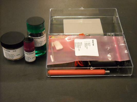
The BEST Gold Contact Replating Kit includes the tools you need for fast replating and modification of circuit contacts. Edge contacts may require replating if they are contaminated with solder or become scratched during handling or do not meet the m
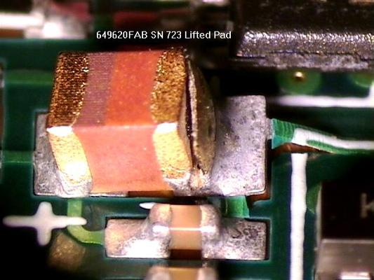
New Equipment | Rework & Repair Services
PCB Repair Services BEST is your experienced resource for high value added PCB repair services. If you need any of the following completed to your printed circuit board then let the experts at BEST be your answer: Pad repair services Pad replace
Electronics Forum | Wed Jun 25 08:50:54 EDT 2003 | russ
I believe that Fancort makes some finger protectors that are made of Metal (Aluminum, titanium, etc...) I don't know how well these would process through placement equipment however due to their thickness. Could you clean the Kapton residue off just
Electronics Forum | Thu Oct 07 20:34:48 EDT 1999 | Tony Huang
Hi, Does anybody know what is the minimum gold plating thickness on the PCB goldfinger required by the industrial specifications - IPC, Bellcore, etc. Where can I find the information? Appreciate for the help! Thanks, Tony
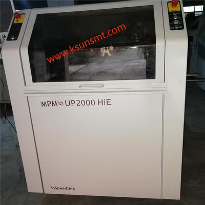
Used SMT Equipment | Screen Printers
MPM UP2000HiE PRINTER Substrate treatment Minimum/maximum size 2"x 2"(50.0 mm x50.0 mm) to 20" x 16" (508 mm x 406 mm)(16 "or larger substrate requires special clamps) Thickness rang
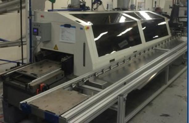
Used SMT Equipment | Soldering - Wave
Model: 6622CC Vintage: 2006 Details: • Windows 7 operating system • Lead Free capable (was running lead, and will need tin wash). • 18” max width adjust • Measured Values Read-out of Frequency controlled motors on PC screen • 400V / 3 Phase
Industry News | 2003-05-19 10:06:43.0
The PCB is available with a maximum panel size of 406-by-460mm and a minimum board thickness of 0.8mm.
Industry News | 2018-10-18 09:06:41.0
Gold Fingers: A Guide to Understanding Gold-Plated PCB Connectors

Parts & Supplies | Soldering - Wave
ELECTROVERT V STYLE, THICK, TITANIUM FINGER PN 3-0257-242-01-03 (EF07)
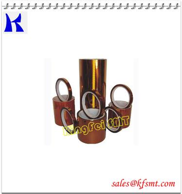
Parts & Supplies | Tape and Reel
SMT Kapton Tape Polymide film tape Specifications: Antistatic Thermally conductive Polyimides for fine line circuitry Cryogenic insulation Corona resistant Pigmented for color Conformable Other films tailored to meet customers needs Param
Technical Library | 2014-08-07 15:13:44.0
Gold embrittlement in SnPb solder is a well-known failure mechanism in electronic assembly. To avoid this issue, prior studies have indicated a maximum gold content of three weight percent. This study attempts to provide similar guidance for Pb-free (SAC305) solder. Standard surface mount devices were assembled with SnPb and SAC305 solder onto printed boards with various thicknesses of gold plating. The gold plating included electroless nickel immersion gold (ENIG) and electrolytic gold of 15, 25, 35, and 50 microinches over nickel. These gold thicknesses resulted in weight percentages between 0.4 to 7.0 weight percent.
Technical Library | 2014-11-06 16:43:24.0
This paper summarizes the results of recent investigations to examine the effect of electroless nickel process variations with respect to Pb-free (Sn-3.0Ag-0.5Cu) solder connections. These investigations included both ENIG and NiPd as surface finishes intended for second level interconnects in BGA applications. Process variations that are suspected to weaken solder joint reliability, including treatment time and pH, were used to achieve differences in nickel layer composition. Immersion gold deposits were also varied, but were directly dependent upon the plated nickel characteristics. In contrast to gold, different electroless palladium thicknesses were independently achieved by treatment time adjustments.
we have many universal gold plus feeders to sell . www.smt-store.com

Safe, precision rework for SMD, BGA, and other high value chips The versatile SV560A rework station combines precision, reliability, and affordability in an all-in-one solution for all your rework needs, from complex, densely populated PCBAs to simpl
Events Calendar | Wed Mar 18 00:00:00 EDT 2020 - Wed Mar 18 00:00:00 EDT 2020 | College Park, Maryland USA
CALCE Reliability Science Symposium - Spring 2020
Career Center | Shen Zhen, China | Management,Sales/Marketing
Working in GLORYPCB for 10 years.knowing electronic supply chain very well. especially for PCB PCBA assembly and other Electronic Manufacturing Service.Glorypcb is a professional electronic manufacturer located in Shenzhen with three facilities.offe
Career Center | Erode, Tamilnadu India | Engineering
Professional Summary 3+ years of experience in the PCB CAM engineering Exposure to FRONTLINE GENESIS 2000 Having exposure in UCAM Exposure to Create, Array & Panelize it for manufacturability Experienced in Creating impedance cou
Gold Wire Bonding Performance and Reliability of ENEPIG Surface Finishes Gold Wire Bonding Performance and Reliability of ENEPIG Surface Finishes The expression "multifunctional PCB", as a synonym for a PCB which is applicable with a variety
| https://www.eptac.com/soldertips/soldertips-gold-removal-and-wave-soldering-vs-hand-soldering/
4.5.1 Gold Removal in J-STD-001 as you had mentioned. The gold has to be removed from component leads whose gold thickness exceeds
Imagineering, Inc. | https://www.pcbnet.com/quote/board-quote-taiwan/
Black Blue Red GoldFingers * Gold Finger Plating Thickness No Gold Fingers 10u" 20u" 30u" 50u" Routing Individual Scoring Route/Retain Route/Retain/Scoring Cutouts/Slots


