Industry Directory | Distributor / Manufacturer
Silver Edge Packaging is offering customers an excellent facility to make their own custom logo with box & style. We are providing best and high quality material packaging with fastest delivery. We facilitate your business by brin
IPS offering full range of ESD and flame-retardive plastic pallets and returnable containers
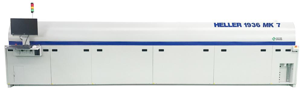
Convection Reflow Oven The World's Best Convection Reflow Oven for High-Throughput The New reflow oven platform revolutionizes the Convection Reflow Oven / Reflow Soldering industry with several new and ground breaking designs! The MK7 convecti
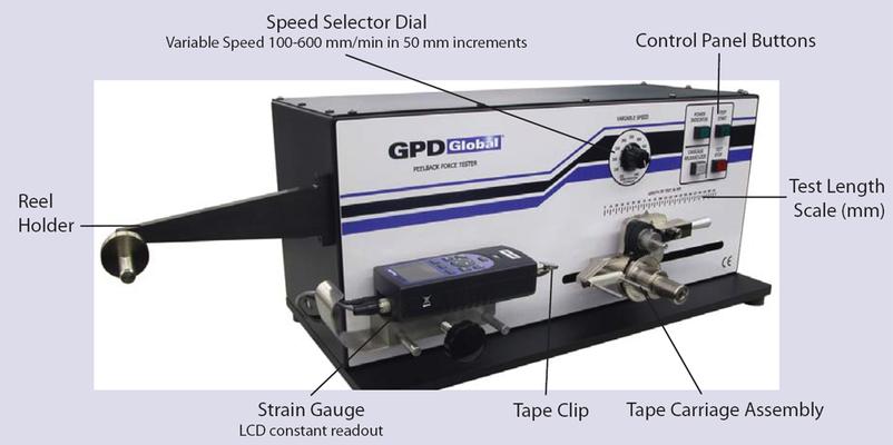
Proven Peel Back Force Measurement Supplying consistent SMT carrier packaging is critical for customers using SMT pick-and-place machines. Nothing will stop a production line faster than carrier cover tape that doesn’t peel back properly. The proble
Electronics Forum | Wed Sep 29 17:36:02 EDT 1999 | Earl Moon
We are all faced with increasing interconnect density in all we do. This means smaller everything, especially components and that which they are mounted upon but, hopefully, without smaller minds and thoughts. It all demands more process control and
Electronics Forum | Thu Sep 30 11:23:41 EDT 1999 | Wolfgang Busko
| We are all faced with increasing interconnect density in all we do. This means smaller everything, especially components and that which they are mounted upon but, hopefully, without smaller minds and thoughts. It all demands more process control an
Used SMT Equipment | Pick and Place/Feeders
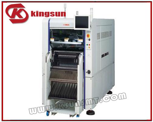
Product number: YS40 Products in detail YSM40 characteristics Integrating "high-speed" and"flexibility" 100000 CPH (IPC9850) high-speedproductivity There are three mount head types to choosefrom Only 1 m wide, small body Wi

Used SMT Equipment | SMT Equipment
Product name: YSM40 high density modular chip mounter Product number: YS40 Products in detail YSM40 characteristics Integrating "high-speed" and "flexibility" 100000 CPH (IPC9850) high-speed productivity There are three mount head types to ch
Industry News | 2013-08-15 20:58:22.0
Heller Industries announced today that they have entered into a joint development agreement with International Business Machines Corporation (NYSE: IBM), to collaborate on the development of fluxless mass reflow furnace equipment and process for high volume manufacturing. The fluxless process utilizes gas phase formic acid to replace standard fluxing agents, and eliminates the need for pre-reflow fluxing and post-reflow flux cleanup steps.
Industry News | 2021-11-08 14:38:39.0
Heller Industries, a leading supplier of reflow soldering ovens for electronic manufacturing and pressure curing ovens for back-end semicondutor manufacturing, today announced they will be exhibiting their new MK7 reflow oven at the San Diego Conference Center January 25-27, 2022.
Parts & Supplies | Pick and Place/Feeders
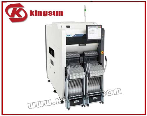
Product number: RX - 7 Detailed product introduction Characteristic With high productivity, versatility, highquality new modular placement machine RX 7 listed Component placement speed (best conditions): 75000 CPH chip components Element size: 0
Technical Library | 2023-01-17 17:58:36.0
Heterogeneous integration has become an important performance enabler as high-performance computing (HPC) demands continue to rise. The focus to enable heterogeneous integration scaling is to push interconnect density limit with increased bandwidth and improved power efficiency. Many different advanced packaging architectures have been deployed to increase I/O wire / area density for higher data bandwidth requirements, and to enable more effective die disaggregation. Embedded Multi-die Interconnect Bridge (EMIB) technology is an advanced, cost-effective approach to in-package high density interconnect of heterogeneous chips, providing high density I/O, and controlled electrical interconnect paths between multiple dice in a package. In emerging architectures, it is required to scale down the EMIB die bump pitch in order to further increase the die-to-die (D2D) communication bandwidth. Aa a result, bump pitch scaling poses significant challenges in the plated solder bump reflow process, e.g., bump height / coplanarity control, solder wicking control, and bump void control. It's crucial to ensure a high-quality solder bump reflow process to meet the final product reliability requirements. In this paper, a combined formic acid based fluxless and vacuum assisted reflow process is developed for fine pitch plated solder bumping application. A high-volume production (HVM) ready tool has been developed for this process.
Technical Library | 2023-01-17 17:12:33.0
Reflowed indium metal has for decades been the standard for solder thermal interface materials (solder TIMs or sTIMs) in most high-performance computing (HPC) TIM1 applications. The IEEE Heterogeneous Integration Thermal roadmap states that new thermal interface materials solutions must provide a path to the successful application of increased total-package die areas up to 100cm2. While GPU architectures are relatively isothermal during usage, CPU hotspots in complex heterogeneously-integrated modules will need to be able to handle heat flux hotspots up to 1000W/cm2 within the next two years. Indium and its alloys are used as reflowed solder thermal interface materials in both CPU and GPU "die to lid/heat spreader" (TIM1) applications. Their high bulk thermal conductivity and proven long-term reliability suit them well for extreme thermomechanical stresses. Voiding is the most important failure mode and has been studied by x-ray. The effects of surface pretreatment, pressure during reflow, solder flux type/fluxless processing, and preform design parameters, such as alloy type, are also examined. The paper includes data on both vacuum and pressure (autoclave) reflow of sTIMs, which is becoming necessary to meet upcoming requirements for ultralow voiding in some instances.

Proven Peel Back Force Measurement Supplying consistent SMT carrier packaging is critical for customers using SMT pick-and-place machines. Nothing will stop a production line faster than carrier cover tape that doesn’t peel back properly. The proble

ACI Technologies Inc. (ACI) is a scientific research corporation dedicated to the advancement of electronics manufacturing processes and materials for The Department of Defense and industry. This video provides an overview of our commercial service
Training Courses | | | Other Courses
Other courses related to electronics manufacturing and assembly
Training Courses | | | PCB Design Courses
The PCB design courses teach students the process, techniques and tools needed to design layout of printed circuit boards.
Events Calendar | Tue Jul 17 00:00:00 EDT 2018 - Wed Jul 18 00:00:00 EDT 2018 | ,
Fan Out Packaging- Technology Overview and Evolution - SMTA Webtorial
Events Calendar | Tue Jun 02 00:00:00 EDT 2020 - Thu Jun 04 00:00:00 EDT 2020 | Markham, Ontario Canada
International Conference for Electronics Hardware Enabling Technologies (ICEHET)
Career Center | Fremont, California USA | Engineering
Interprets electrical design requirements and uses Allegro design tool to create original PCB layouts, detailed fab drawings, schematics, and other design files. Work with HW design engineer to make sure PCB layout meet PCB design requirements.
Career Center | Fremont, California USA | Engineering
Job Description: • Has full ownership of HW design and release including HW specification creation, schematic generation, PCB layout, board bring up, and design verification. • Complete PCB design schematic using Orcad capture. • Complete HW desig
Career Center | GOBICHETTIPALAYAM, India | Engineering
PCB design, layout and packaging of high-speed, high-density, Mixed Technology Analog / Digital signals & RF signals, Flex, Rigid board, Commercial, Application Boards, based on client requirement and Quality Inspection of the design.
SMTnet Express, March 1, 2018, Subscribers: 31,280, Companies: 10,908, Users: 24,452 Deposition of Solder Paste into High Density Cavity Assemblies Fernando Coma, Jeffrey Kennedy, Thilo Sack; Celestica Corporation Circuit functional density
| https://www.smtxtra.com/news-events/page/3/
. Our specialist team will provide information about our company, the high-quality products we can supply and the services we can offer to meet your Company budgets. Join us at Bitec, Bangkok, 22nd


