Industry Directory | Manufacturer
US manufacturer of metallized ceramic substrates & packages; specializing in PCTF (plated copper over thick film) & low cost AgENIG (silver with electroless nickel and immersion gold plating).
Industry Directory | Manufacturer
2Layers - 18Layers ;HASL, OSP, Gold plating, immersion Gold/Silver/Tin, removable mask, gold-finger, carbon ink;Conact Person:Rene E-mail:rene@speedingcircuit.com Website:www.speedingcircuit.com
New Equipment | Assembly Services
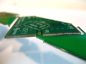
- 6 layer with immersion silver finish. - Plating on the edges. Advantages: - Special plating to ensure plating remains on the edges of the board. - 3~6 working days for prototypes, for prototype production. Edge Plating The requirement for edge p
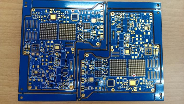
1~26 layers, High Mix low volume to Mass production. FR4-Tg140~200. Surface finish OSP, Immersion gold, Immersion silver, Immersion tin, Hard gold plating etc. Finish copper up to 6oz. HDI 2+N+2 Capability.
Electronics Forum | Thu Jun 16 17:02:40 EDT 2011 | boardhouse
The finish looks like Immersion Tin or Silver. if its lead free Hot air - could be issue of to high of a Tin Content. find out what brand of Hasl they are using. SL100 Example. Is this tarnished look only being seen after assembly or have you seen
Electronics Forum | Sat Sep 20 07:11:28 EDT 2008 | Sean
Hello All, I used to hear that PCB with immersion silver finishing, its non component location pads, tend to be discolour (Yellowish) after went through heat cycle, such as reflow oven. However, if the component solderbility on the PCB is OK, can w
Industry News | 2010-09-13 15:36:15.0
IPC — Association Connecting Electronics Industries® has released IPC-1601, Printed Board Handling and Storage Guidelines. The industry's sole standard on the handling, packaging and storage of printed boards, IPC-1601 provides users with guidance on how to protect printed boards from contamination, physical damage, solderability degradation, electrostatic discharge and moisture uptake.
Industry News | 2018-10-18 10:16:53.0
Solder Tinned Pads vs Gold Plated Pads - The Importance of Selecting the Proper Surface Finish
Technical Library | 2023-08-04 15:27:30.0
A designed experiment evaluated the influence of several variables on appearance and strength of Pb-free solder joints. Components, with leads finished with nickel-palladium-gold (NiPdAu), were used from Texas Instruments (TI) and two other integrated circuit suppliers. Pb-free solder paste used was tin-silver-copper (SnAgCu) alloy. Variables were printed wiring board (PWB) pad size/stencil aperture (the pad finish was consistent; electrolysis Ni/immersion Au), reflow atmosphere, reflow temperature, Pd thickness in the NiPdAu finish, and thermal aging. Height of solder wetting to component lead sides was measured for both ceramic plate and PWB soldering. A third response was solder joint strength; a "lead pull" test determined the maximum force needed to pull the component lead from the PWB. This paper presents a statistical analysis of the designed experiment. Reflow atmosphere and pad size/stencil aperture have the greatest contribution to the height of lead side wetting. Reflow temperature, palladium thickness, and preconditioning had very little impact on side-wetting height. For lead pull, variance in the data was relatively small and the factors tested had little impact.


