Industry Directory | Manufacturer / Other
OEM Contract Manufacturer, Prototype production, battery testing, quick turn production, high/Low volume production. OEM products, complete box build, sub assembly, battery chargers, power supplies, microphones, cable and flex assembly.
New Equipment | Rework & Repair Services
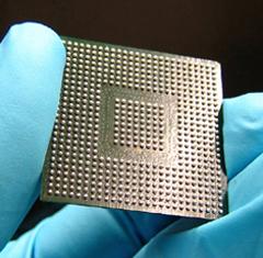
BGA Rework Services Offered BGA Remove and Placement Level Three Pad Repair Wire Add Trace Repair BGA Re-Balling BGA Inspection We Rework PBGA (Plastic Ball Grid Array) TBGA (Tape Ball Grid Array) uBGA (Micro BGA) CCGA (Ceramic Colum
New Equipment | Rework & Repair Services
Reliable LGA Rework Services to Rescue Your Project BEST is your source for LGA rework services. We can optimize our processes to make sure voiding is minimized and the interconnection to all of the IO meets the IPC classification for the assembly.
Electronics Forum | Fri Mar 30 23:35:43 EDT 2007 | mika
Question: Does this formula apply even for the small LGA:s like LGA36 6.5 x 3.5 x 0.6 mm pad size 0.35mm pitch 0.60mm? We use a 0.13 mm stencil thichess beacuse on the same board there is some P.I.P comps. The board dimensions is 35 x 50 mm on a pane
Electronics Forum | Mon Aug 10 12:28:17 EDT 2009 | davef
We don't know dip about your Linear Tech LGA118, but we agree with published reports that say you should have between 4800 and 7000 thou^3 of paste on the pad for a LGA. These volumes were analyzed based on volumes found successful for CGA and then e
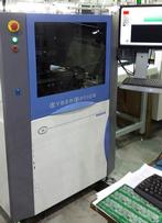
Used SMT Equipment | SPI / Solder Paste Inspection
Vintage: 2008 Description: 3D Solder Paste Inspection Details: • 3D sensing system w/ built-in fiducial camera and lighting • MicroPad Sensor • Mechanical board stop • Auto-width adjust conveyor • Max PCB width: 20” x 20” • Max inspection
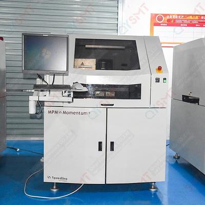
Used SMT Equipment | Screen Printers
Substrate processing: Maximum substrate size (XxY): 609.6mmx508mm(24”x20”) For circuit boards larger than 20”, special fixtures are required Minimum substrate size (XxY): 50.8mmx50.8mm(2”x2”)
Industry News | 2009-04-23 20:54:01.0
MINNEAPOLIS, MN � The SMTA is pleased to announce its latest technical event in Penang, Malaysia. The SMTA South East Asia Technical Conference on Electronics Assembly Technologies will be held November 19-20, 2009 at the Equatorial Hotel in Penang, Malaysia. Presentations are currently being solicited for the following key technology tracks:
Industry News | 2016-09-22 17:27:09.0
IPC — Association Connecting Electronics Industries® invites researchers, technical experts and industry leaders to submit abstracts for poster presentations at IPC APEX EXPO®, the industry’s premier conference and exhibition for printed board design and manufacturing, electronics assembly and test. Poster presentations are scheduled for Wednesday, February 15, 2017, and will be displayed throughout the event, offering additional visibility.
.jpg)
Parts & Supplies | SMT Equipment
We also supply following Panasonic Spare parts : KXFB02GBC06 FRAME KXFB05CGA01 BOLT N210009258AA PLATE KXFB02GJA00 BLOCK KXFB02GKA00 BLOCK N210018293AA COVER N210018294AA COVER N210018299AA COVER KXFB02NSA00 BRACKET KXFB02NVA00 DOG KXFB02
Parts & Supplies | Circuit Board Assembly Products
PULANG TECHNOLOGY CO,.LTDOffers electronic manufacturing services including PCB designing, electronic contract manufacturing including electronic product design, electronic product development, electronic product repair, PCB manufacturing, electronic
Technical Library | 2019-04-17 21:29:14.0
Electroless nickel electroless palladium immersion gold (ENEPIG) surface finish for printed circuit board (PCB) has now become a key surface finish that is used for both tin-lead and lead-free solder assemblies. This paper presents the reliability of land grid array (LGA) component packages with 1156 pads assembled with tin-lead solder onto PCBs with an ENEPIG finish and then subjected to thermal cycling and then isothermal aging.
Technical Library | 2015-07-14 13:19:10.0
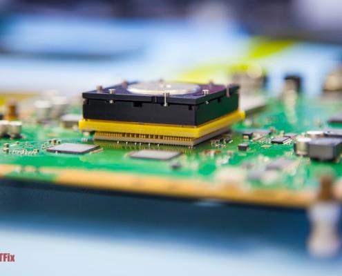
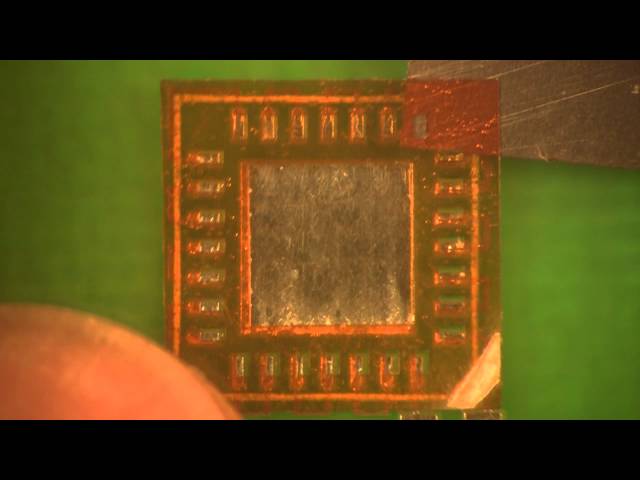
Bottom terminated components (BTC) are leadless components where terminations are protectively plated on the underside of the package. They are all slightly different and have different names, such as QFN (quad flat no lead), DFN (dual flat no lead), LGA (land grid array) and MLF (micro lead-frame. BTC assembly has increased rapidly in recent years. This type of package is attractive due to its low cost and good performance like improved signal speeds and enhanced thermal performance. However, bottom terminated components do not have any leads to absorb the stress and strain on the solder joints. It relies on the correct amount of solder deposited during the assembly process for having a good solder joint quality and reliable reliability. Voiding is typically seen on the BTC solder joint, especially on the thermal pad of the component. Voiding creates a major concern on BTC component’s solder joint reliability. There is no current industry standard on the voiding criteria for bottom terminated component. The impact of voiding on solder joint reliability and the impact of voiding on the heat transfer characteristics at BTC component are not well understood. This paper will present some data to address these concerns.
Substrate processing: Maximum substrate size (XxY): 609.6mmx508mm(24”x20”) For circuit boards larger than 20”, special fixtures are required Minimum substrate size (XxY): 50.8mmx50.8mm(2”x2”)
Training Courses | | | PCB Rework and Hand Soldering Courses
The PCB rework and hand soldering courses courses cover techniques of rework and repair of PCBs, BGAs and other electronics assemblies, and teach fundamentals of soldering of electronics assemblies.
Training Courses | | | PCB Rework and Hand Soldering Courses
The PCB rework and hand soldering courses courses cover techniques of rework and repair of PCBs, BGAs and other electronics assemblies, and teach fundamentals of soldering of electronics assemblies.
ORION Industries | http://orionindustries.com/pdfs/gappad.pdf
. * Graphs and data generated from Young's Modulus, calculated using 0.01 inch/min. step rate of strain with a sample size of 0.79 inch2. MODULUS * The modulus of Gap Pad VO is rate dependent due to its viscoelastic properties
| http://etasmt.com:9060/te_news_industry/2021-09-15/26566.chtml
Size Does Matter – Breaking the Barriers of Wafer Level Packaging-SMT Technical-Reflow oven,SMT Reflow Soldering Oven-cmsadmin Home About


winsouce.jpg)
.png)