Industry Directory | Manufacturer
MIRTEC has earned a solid reputation as one of the most Progressive and Dynamic Suppliers of Automated SMT Inspection Equipment to the Electronics Manufacturing Industry.
Industry Directory | Manufacturer
A worldwide leader in Automated Optical and X-ray Inspection
SUPERIOR VISION 6000 � UNRIVALED SOLDER DEFECT DETECTION The Photon Dynamics Superior Vision (SV) 6000 AOI system delivers comprehensive defect detection. Designed for high-pulse production of large-format, high-density and small component PWAs,
SUPERIOR VISION 4000 � SUPERIOR SOLDER DEFECT DETECTION The Photon Dynamics Superior Vision (SV) 4000 AOI system delivers comprehensive defect detection. Designed for high-pulse production of large-format, high-density and small component PWAs, t
Electronics Forum | Sun Aug 09 15:25:17 EDT 2015 | dev88
dear sir i am new for aoi section,my work will be teaching of aoi defect and related to programming, want to know how to make program easily in mirtec 4.1.1 and what are the different standard which we must understand.
Electronics Forum | Tue Nov 06 06:23:31 EST 2007 | clampron
Good Morning Roger, The Mirtec's can be adjusted to lower your false call rate. This can be done by reducing the matching percentage for each componnent but the result of this action is that the machine becomes less selective. If you lower them too
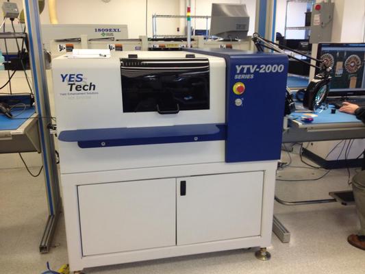
Used SMT Equipment | AOI / Automated Optical Inspection
Capture on the fly technology 3D Fusion Lighting (RGB+White LED's) 5 megapixel color imaging 2 top-down and 4 side angle cameras Quick set-up High speed, high defect coverage Low false failure rate Programmable conveyor for boards up to 20 x 2
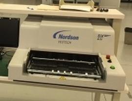
Used SMT Equipment | AOI / Automated Optical Inspection
5 megapixel color imaging / (1) top-down and (4) side angle cameras / quick set-up / high speed / high defect coverage / low false failure rate Complete and Operational USA / FOB Origin Immediate
Industry News | 2015-08-24 14:59:01.0
MIRTEC, “The Global Leader in Inspection Technology,” announces that it will exhibit in Booth #407 at SMTA International, scheduled to take place Sep. 29-30, 2015 at the Donald Stephens Convention Center in Rosemont, IL. Company representatives will showcase the latest advancement MIRTEC’s award-winning 3D AOI and SPI systems during the two-day event.
Industry News | 2016-05-03 14:36:37.0
MIRTEC, “The Global Leader in Inspection Technology,” is pleased to announce that it was awarded the 2016 EM Asia Innovation Award in the category of Inspection & Testing – AOI for its MV-6 OMNI 3D AOI system. The award was presented to the company during a ceremony that took place April 26, 2016 at the Shanghai World Expo Exhibition & Convention Center during NEPCON China. MIRTEC’s MV-6 OMNI also earned the top score in the AOI category, resulting in an SMT China Vision Excellence Award.

Parts & Supplies | SPI / Solder Paste Inspection
Quick programming, friendly programming interface Multiple measurement methods True one-button measurement Eight-way motion button, one-click focus Adjustable scanning pitch Solder paste 3D simulation function Powerful SPC function MARK
Parts & Supplies | Soldering Equipment/Fluxes
3D Solder Paste Inspection Machine Features : Easy to use by fully motorize X-Y scan mechanism. Easy to program by Gerber image navigator Easy to repeat the same job by loading the saved program User-friendly color image live view operation Ea
Technical Library | 2022-06-27 16:50:26.0
Electronics industry is one of the fastest evolving, innovative, and most competitive industries. In order to meet the high consumption demands on electronics components, quality standards of the products must be well-maintained. Automatic optical inspection (AOI) is one of the non-destructive techniques used in quality inspection of various products. This technique is considered robust and can replace human inspectors who are subjected to dull and fatigue in performing inspection tasks. A fully automated optical inspection system consists of hardware and software setups. Hardware setup include image sensor and illumination settings and is responsible to acquire the digital image, while the software part implements an inspection algorithm to extract the features of the acquired images and classify them into defected and non-defected based on the user requirements. A sorting mechanism can be used to separate the defective products from the good ones. This article provides a comprehensive review of the various AOI systems used in electronics, micro-electronics, and opto-electronics industries. In this review the defects of the commonly inspected electronic components, such as semiconductor wafers, flat panel displays, printed circuit boards and light emitting diodes, are first explained. Hardware setups used in acquiring images are then discussed in terms of the camera and lighting source selection and configuration. The inspection algorithms used for detecting the defects in the electronic components are discussed in terms of the preprocessing, feature extraction and classification tools used for this purpose. Recent articles that used deep learning algorithms are also reviewed. The article concludes by highlighting the current trends and possible future research directions.
Technical Library | 2024-04-29 21:39:52.0
In this paper, we develop and put into practice an Automatic Optical Inspection (AOI) system based on machine vision to check the holes on a printed circuit board (PCB). We incorporate the hardware and software. For the hardware part, we combine a PC, the three-axis positioning system, a lighting device and CCD cameras. For the software part, we utilize image registration, image segmentation, drill numbering, drill contrast, and defect displays to achieve this system. Results indicated that an accuracy of 5µm could be achieved in errors of the PCB holes allowing comparisons to be made. This is significant in inspecting the missing, the multi-hole and the incorrect location of the holes. However, previous work only focusses on one or other feature of the holes. Our research is able to assess multiple features: missing holes, incorrectly located holes and excessive holes. Equally, our results could be displayed as a bar chart and target plot. This has not been achieved before. These displays help users analyze the causes of errors and immediately correct the problems. Additionally, this AOI system is valuable for checking a large number of holes and finding out the defective ones on a PCB. Meanwhile, we apply a 0.1mm image resolution which is better than others used in industry. We set a detecting standard based on 2mm diameter of circles to diagnose the quality of the holes within 10 seconds.
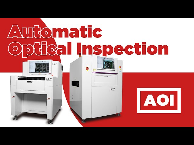
I.C.T Provide SMT Production Line solutions with Automated Optical Inspection (AOI) AOI is short for Automated Optical Inspection, which is widely used in the electronics industry to check the appearance of PCBA assembly at the back end of the cir
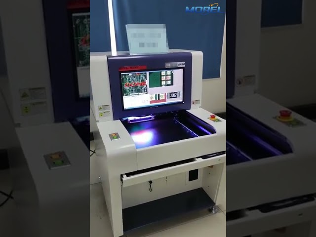
ML-A410 SMT Automated Optical Inspection Machine Feature ▶Economical and practical AOI. ▶High precision detection platform design. ▶Fast programming debugging integration. ▶Automatic recognize the Tip and Bottom side. ▶Professional SPC system.
Events Calendar | Mon Apr 23 00:00:00 EDT 2018 - Thu Apr 26 00:00:00 EDT 2018 | Shanghai, China
SMTA China East Conference 2018
Career Center | Wellsboro, Pennsylvania USA | Engineering
SMT PROCESS ENGINEER: (Wellsboro, PA) - Designs, defines and plans the manufacturing process. Specifies and directs installation of new processes. Plans equipment build schedules and monitors vendor progress. Defines and recommends equipment, methods
Career Center | seoul, South Korea | Engineering
I have 4 year process engineering in Motorola and 7 years service experience in Assemblen . 2 years in Mirtec AOI as service manager .
Career Center | Grand Prairie, Texas USA | Production,Quality Control,Technical Support
SMT Programmering Specialist. Pick and place, screen printer, AOI and quality inspection, process control, CAD and program development.
SMTnet Express, April 21, 2022, Subscribers: 25,664, Companies: 11,565, Users: 27,188 Deep Learning Based Defect Detection for Solder Joints on Industrial X-Ray Circuit Board Images Quality control is of vital importance during
SMTnet Express August 8, 2013, Subscribers: 26202, Members: Companies: 13446, Users: 35028 Automatic PCB Defect Detection Using Image Substraction Method by Sonal Kaushik, Javed Ashraf; Al-Falah School of Engineering & Technology A printed circuit
winsouce.jpg)
.gif)

.gif)
