Industry Directory | Manufacturer
US manufacturer of metallized ceramic substrates & packages; specializing in PCTF (plated copper over thick film) & low cost AgENIG (silver with electroless nickel and immersion gold plating).
Industry Directory | Manufacturer
Manufacturer of advanced process chemistry for plating, masking and stripping. Custom manufacturing of automated equipment for electrodeposion including; hoist systems, reel-to-reel and continuous vertical processing equipment.
New Equipment | Fabrication Services
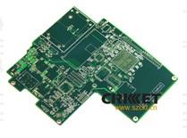
Base Material: FR4 Layer count: 4 layer Board thickness: 1.6mm Copper Thickness:1 oz Surface finish: nickel gold plating Soldermask Colors: Green Size:159.25*182/1up
Double-Sided & Multi-Layer PCB Material: - FR-4 / Hi-Temp FR-4 / FR-5 / G10 / BT / Polyimide - Very Thin PCB: 0.004" 2L ~ 0.030" 8L - Thick Copper: 1/4 oz. ~ 11 oz. Process: - PTH - Blind/Buried/Segmented Via - Sequential Lamination - MicroVia Capa
Electronics Forum | Thu Jul 15 06:27:50 EDT 2010 | xps
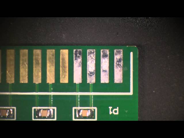
Hi after an enviromental test 85C/85RH, for 3 months (powered), of an electronic assembly with edge finger tabs ENIG finished (nickel 5micron, gold 0.02micron), the nickel disappears completely under the gold (due to corrosion, I think). Does anyone
Electronics Forum | Thu Jul 15 13:27:42 EDT 2010 | xps
Thanks... anyway I confirm, the nickel disappear (verified by cross section)and a strange substance greyish above gold, covering the tabs after test. I don't know the reason for this phenomenon. I don't believe that with proper electrolytic nickel fi
Industry News | 2003-05-19 10:06:43.0
The PCB is available with a maximum panel size of 406-by-460mm and a minimum board thickness of 0.8mm.
Industry News | 2003-04-09 08:25:50.0
A new design guide is available from Genalog detailing Samtec's flex circuit capabilities.
Parts & Supplies | Circuit Board Assembly Products
1) 160*100mm, FR-4 CTI ≥ 600V 2) 8 layer impedance control 3) Copper weight(finished inner/outer): 1 oz 4) LPI Green mask/white silk 5) Min hole 0.19mm, 5/3 track/gap 6) 1.6mm +/-10% thick 7) Immersiong gold over nickel
Parts & Supplies | Circuit Board Assembly Products
1). 1+C+1 HDI, buried/blind L1-L5/L5-L8 vias. 2). FR-4 Material, 1 oz weight. 3). 8 layer, 1.6mm thick. 4). 4/4 mils track and space 5). Min.drill 0.1mm 6). Green solder mask/ white silkscreen 7). Immersion gold over nickel
Technical Library | 2019-06-04 10:19:46.0
Interconnection technology relies very heavily on the ability of the conductors on a printed wiring assembly to maintain reliable signal integrity. Harsh environmental factors can precipitate a loss of conductivity due to oxidation and corrosion. Connections are typically soldered or inserted using pressure fitted connectors to obtain enough surface contact to meet the electrical conductivity requirements. In pressure contacts, surface integrity is especially critical where the abrasive effects of retraction and insertion can wear off the metallic finish from the contact area. This can expose the underlying copper or nickel and lead to increased resistance at the contact points. These types of conductors are frequently found in card edge connectors where the terminations are plated with a layer of nickel and gold (frequently referred to as gold fingers). A hard gold is typically used containing very small amounts of nickel and cobalt to increase the wear resistance.
Technical Library | 2019-06-07 14:49:54.0
ACI Technologies was contacted in regards to poor solder joint reliability. The customer submitted an assembly that was exhibiting intermittent opens at multiple locations on a ball grid array (BGA) component. The assembly’s functionality did not survive international shipping, essentially shock and vibration failures, immediately making the quality of the solder joints suspect. The customer was asked about the contract manufacturer and the reflow oven profile as well as the solder paste and surface finish used. The ACI engineering staff evaluated the contract manufacturer’s technique and determined that they were competent in the methods they used for placing thermocouples in the proper locations and developing the reflow oven profile. The surface finish was unusual, but not unheard of, in that it was hard gold over hard nickel, rather than electroless nickel immersion gold (ENIG). The customer was able to supply boundary scan testing data which showed a diagonal row of troublesome BGA pins.

ACI Technologies Inc. (ACI) is a scientific research corporation dedicated to the advancement of electronics manufacturing processes and materials for The Department of Defense and industry. This video provides an overview of our commercial service
BEST Inc master instructor Norman Mier demonstrates how to replate gold fingers using the BEST gold contact replating kit. In this video he demonstrates how to repair, prepare and replate the finger using a gold replating solution. If you want to lea
Events Calendar | Wed Apr 20 00:00:00 EDT 2022 - Wed Apr 20 00:00:00 EDT 2022 | ,
Virtual Course: Selection Criteria of Surface Finish for Next Generation PCB Technologies
Events Calendar | Tue Jan 23 00:00:00 EST 2018 - Tue Jan 23 00:00:00 EST 2018 | New Milford, Connecticut USA
FREE Webinar: Eliminate Circuit Board Problems and Failure Modes
SMTnet Express, August 7, 2014, Subscribers: 23058, Members: Companies: 13975, Users: 36604 Gold Embrittlement In Lead-Free Solder. Craig Hillman, Nathan Blattau, Joelle Arnold, Thomas Johnston, Stephanie Gulbrandsen; DfR Solutions , Julie Silk
PCB Libraries, Inc. | https://www.pcblibraries.com/forum/top-10-smt-new-product-stories-of-2014_topic1520_post6150.html
#2, BEST Intros Nickel Gold Repair Circuit Frames: BEST Inc. is pleased to announce the availability of nickel gold circuit frames
Imagineering, Inc. | https://www.pcbnet.com/blog/everything-you-need-to-know-about-pcb-finish/
: nickel and gold, and hot air solder leveling (HASL). Today, dozens of options for PCB finishes are available, each with their own benefits for different applications


