New Equipment | Rework & Repair Services
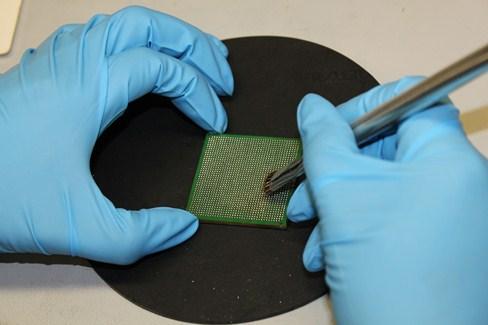
BGA Reballing Services BEST provides BGA reballing services for your plastic-, ceramic- and metalbodied components down to 0.3mm pitch. We have the ability to develop the BGA reballing process you want with a variety of deballing methods and machine

New Equipment | Assembly Services
Quick turn Prototype PCBs from 24 hour turnaround to high volume printed circuit board production from our domestic plant in USA and/or China facilities. Our Modern 38,000 sq. ft. manufacturing plant with multi-million dollar investment with latest e
Electronics Forum | Fri Jan 22 16:03:17 EST 2021 | SMTA-64387124
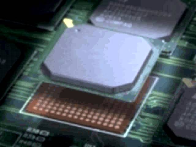
Does anyone see any issues in mixing SMD and NSMD pads within one BGA footprint. We have high current pads which we want to make SMD and the other signal pads to be NSMD
Electronics Forum | Fri Jan 29 16:17:13 EST 2021 | donnie15
The impact is low on larger pitches and pad sizes. as things get to the .4mm pitch the pad differences start affect your ball size and yields. The trace size going into the pads and the solder mask relief can cause some odd shaped pads with signif
Industry News | 2018-10-18 10:40:04.0
Via Tent-Holes with Solder Mask
Industry News | 2018-10-18 08:21:10.0
How to Prevent Non-Wetting Defect during the SMT Reflow Process
Technical Library | 2008-04-08 17:42:27.0
Concern about the failure of lead-free BGA packages when portable devices such as cell phones are accidentally dropped and a general concern about the resistance of these packages under shock loading has prompted an interest in the impact strength of the soldered BGA connection. This paper reports the results of the measurement of the impact strength of lead-free 0.5±0.01mm diameter BGA spheres on 0.42mm solder mask defined pads on copper/OSP and ENIG substrates using recently developed equipment that can load individual BGA spheres at high strain rates in shear and tension.
Technical Library | 2019-08-14 22:20:55.0
Cleanliness is a product of design, including component density, standoff height and the cleaning equipment’s ability to deliver the cleaning agent to the source of residue. The presence of manufacturing process soil, such as flux residue, incompletely activated flux, incompletely cured solder masks, debris from handling and processing fixtures, and incomplete removal of cleaning fluids can hinder the functional lifetime of the product. Contaminates trapped under a component are more problematic to failure. Advanced test methods are needed to obtain "objective evidence" for removing flux residues under leadless components.Cleaning process performance is a function of cleaning capacity and defined cleanliness. Cleaning performance can be influenced by the PCB design, cleaning material, cleaning machine, reflow conditions and a wide range of process parameters.This research project is designed to study visual flux residues trapped under the bottom termination of leadless components. This paper will research a non-destructive visual method that can be used to study the cleanability of solder pastes, cleaning material effectiveness for the soil, cleaning machine effectiveness and process parameters needed to render a clean part.

This video describes the BEST BGA rework and BGA rework services capabilities. What is described in this movie are the people, processes and tools unique to BEST and how that impacts its customers. The advanced equipment set including multiple refl
Training Courses | | | PCB Assembly Courses
The PCB assembly courses provide knowledge of different processes and equipment used in TH and SMT assembly of printed circuit boards.
GPD Global | https://www.gpd-global.com/co_website/fluid-dispense-adhesive-application.php
. For the most part, conductive adhesives are not reworkable like a solder paste connection. Non-Conductive Adhesive is used for holding a device to a substrate without an electrical connection or can be used as an insulator between pads
ASYMTEK Products | Nordson Electronics Solutions | https://www.nordson.com/en/divisions/efd/resource-center/solder-glossary-of-terms
). Bridging Formation of a solder alloy connection between two or more adjacent contacts. Bumped Circuit Boards Bare printed circuit boards that have had solder paste deposited and reflowed on the pads prior to component installation