

Industry Directory | Manufacturer
COT specializes in high quality SMT nozzles and consumables for pick and place machines. We provide special engineering design service of custom nozzles for those unique and odd components.

Industry Directory | Distributor / Manufacturer
Midwest Circuit Technology provides Carbide Router Bits and End Milling Cuters for use in PCB Depaneling equipment. We have over 35 years of supplying tools and machining experience in drilling, Routing, Test Fixture manufacture.
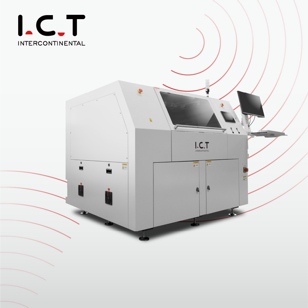
New Equipment | Test Equipment
I.C.T A40 Flying Probe Tester: High-Speed, Precision PCB Inspection The I.C.T A40 Flying Probe Tester is an advanced inspection system designed for high-speed, precise analysis of manufacturing defects on assembled circuit boards. Leveraging cutting
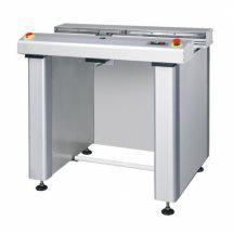
New Equipment | Board Handling - Conveyors
Second-ranking double rack/gear adjustable wide organization, ensure transportation guide mutual parallel; > Machine adopts professional wear-resisting anti-static belts, special aluminum guide rail, ensure smooth shuttle smooth, transportation; >
Electronics Forum | Thu Nov 13 09:27:21 EST 2008 | cisridn
I have tried covering the vias with thermal tape and that did not work. I like the idea of plugging the via with a temporary solder mask. I will try that the next time I build a fixture which should be tomorrow. This is mainly a problem only becau
Electronics Forum | Wed Nov 12 13:00:58 EST 2008 | cisridn
I have to build test fixtures for RF Power transistors. These components generate alot of heat so the PCB is soldered to a baseplate. The problem I am having is that I am getting too much solder flowing thru the via's and flooding the topside of th
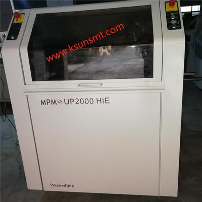
Used SMT Equipment | Screen Printers
MPM UP2000HiE PRINTER Substrate treatment Minimum/maximum size 2"x 2"(50.0 mm x50.0 mm) to 20" x 16" (508 mm x 406 mm)(16 "or larger substrate requires special clamps) Thickness rang
Used SMT Equipment | In-Circuit Testers
• Modular upgrade options from MDA to ICT and functional test • High fault coverage test solution • Limited access solution and functional test expansion using PXI modules • Friendly UI with fast and easy program development.
Industry News | 2003-06-12 08:24:37.0
An adaptive tool prevents small and/or light components "lifting" or "floating" on printed circuit board assemblies during the wave solder process.
Industry News | 2003-04-03 08:51:07.0
Symphony 3070TM Package from JTAG Technologies for Testing and In-System Flash / PLD Programming
Parts & Supplies | Assembly Accessories
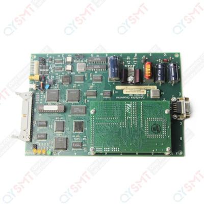
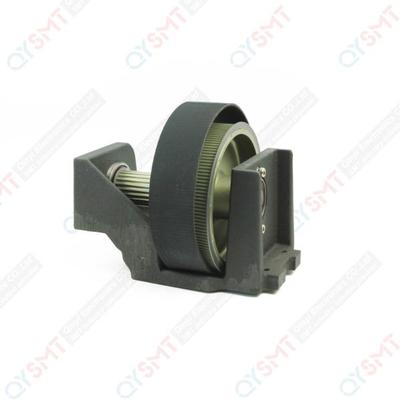
Email= happy@qy-smt.com Wechat= hpy246322 Skype= h4happyraj Website- www.qy-smt.com Contact us for all original New, Copy new and Original used Items. ------------------------------------ 40000625 OPTION LIGHT UNIT 40000627 OP CAMERA ASSY
Parts & Supplies | Assembly Accessories
Email= happy@qy-smt.com Wechat= hpy246322 Skype= h4happyraj Website- www.qy-smt.com Contact us for all original New, Copy new and Original used Items. ------------------------------------ 40000622 ST CAMERA ASSY(HC) 40000625 OPTION LIGHT
Technical Library | 2021-09-02 08:17:07.0
We are a professional manufacturer of PCB depaneling machines, which is workable for all boards, including flex and regid boards, v-scored boards and routed boards. Laser pcb depaneling is non-contact way without mechanical stress,this solution is good for modern precision PCB depaneling. It has below advantages: 1. No dust The production environment of the circuit board industry is carried out in the dust-free workshop. The traditional pcb depaneling equipment, such as blade moving type machine, will inevitably produce residues and micro powder, which will pollute the 10000 and 1000 class dust-free workshops and affect the conductivity of products. The UV laser PCB cutting machine is a vaporization processing process, which will not produce dust and is conducive to the conductivity of the product. 2. High cutting precision The processing gap of high-precision traditional processing equipment can not reach the gap width of less than 100 microns, which will cause certain damage to the lines on the edge or PCBA circuit board containing components. The focus spot of the laser cutting machine is small, and the ultraviolet cold processing mode has little thermal impact on the edge of the circuit board. The cutting position accuracy is less than 50 microns, and the cutting size accuracy is less than 30 microns, which will not affect the edge of the circuit board, and the precision is high. 3. No stress Traditional processing methods generally have V-grooves, which will cause certain damage to the board in the manufacturing process. The UV laser PCB cutting machine can directly cut the bare board without making V-grooves. In addition, the traditional processing methods directly use tools to act on the circuit board, especially the stamping method has a great impact on the circuit board, which is easy to cause board deformation. The laser cutting machine is a non-contact processing mode, which acts on the surface of the material through the high-energy beam, which will not cause the influence of stress and the deformation and damage of the circuit board. 4. For special-shaped cutting, it is easy to automate The UV laser PCB cutting machine can cut for any shape without replacing any props and fixtures, and without steel mesh. The same equipment can meet special-shaped and straight-line cutting, which is easy to realize assembly line automatic production and high flexibility. It is easy to improve production efficiency and save production process and production cycle. In particular, it can quickly and efficiently meet the needs of rapid proofing, directly import the drawing, and then locate the cutting. 5. High compatibility The UV laser PCB cutting machine can process the materials around the circuit board, such as PCB, FPC, covering film, pet, reinforcing board, IC, ultra-thin metal cutting, etc. it has strong practicability, is compatible with the processing of a variety of materials, is easy to operate, can be imported into the drawing, does not need to adjust any mechanical parts, and is easy to operate and maintain. 6. Good cutting edge effect The cutting edge is smooth and neat without burr. It can be processed and formed directly according to the size of the drawing, which is conducive to improving the yield of the product. It can be directly installed into the subsequent process without further processing. For more details about UV laser depaneling, please feel free to contact us. www.pcbdepanelingrouter.com
Technical Library | 2021-05-20 13:55:14.0
Quality Control is essential in production processes. In the PCB Assembly process there are several Quality Control steps or options. The most popular tests are the electrical (In-Circuit or ICT) and the function (functional or FCT/FVT) test. ICT test fixtures are standardized and there are several major test platforms available which are industry standards. For FCT applications there are many more variations possible due to the vast number of testers and interface approaches unique to each customer; also due to an endless list of applications which fall under the category of Functional Test (RF, High Current, LED test, Leak test etc.) Test Probes are a very important part in ICT as well as in FCT applications. If the wrong test probe (type, spring force, tip style etc.) is used, the test fixture will not work as intended. In addition the test probe must be installed correctly in order to work properly. This presentation will show general information and some guidelines for a proper Test Fixture design to assure the most efficient production.

www.unisoft-cim.com/pcbtest.htm - In minutes the Unisoft ProntoTEST-FIXTURE software translates CAD & BOM files into real reference designators, netlists, X/Y component pin geometries, values, tolerances, part numbers, etc. This data is used by Test

http://www.pcb-separator.com/plus/view.php?aid=85 pcb depaneling router/Cnc pcb depanelizer/??????????? ???????? ????/??????/PCB CNC Milling Machine/pcb milling separator/PCB cutter/cnc PCB cutter/CNC separator
Training Courses | | | PCB Rework and Hand Soldering Courses
The PCB rework and hand soldering courses courses cover techniques of rework and repair of PCBs, BGAs and other electronics assemblies, and teach fundamentals of soldering of electronics assemblies.
Training Courses | | | PCB Rework and Hand Soldering Courses
The PCB rework and hand soldering courses courses cover techniques of rework and repair of PCBs, BGAs and other electronics assemblies, and teach fundamentals of soldering of electronics assemblies.
Events Calendar | Wed Oct 02 00:00:00 EDT 2019 - Wed Oct 02 00:00:00 EDT 2019 | ,
3D PCB Design and Analysis, When ECAD Meets MCAD
Career Center | Tampa, Florida USA | Production
Help Reptron Electronics be a leader in the Electronics industry by acting as the Process Engineering Technician on 2nd Shift for our Printed Circuit Board Manufacturing Division in Tampa, Florida. Reptron is a large contract manufacturer providing s
Career Center | Tampa, Florida USA | Engineering,Maintenance,Production,Technical Support
Help Reptron Electronics be a leader in the Electronics industry by acting as the Process Engineering Technician on 2nd Shift for our Printed Circuit Board Manufacturing Division in Tampa, Florida. Reptron is a large contract manufacturer providing s
Career Center | Appleton, Wisconsin USA | Engineering,Production,Research and Development,Technical Support
I have more than 25 years of experience in electronics manufacturing and printed circuit board (PCB) structural test. My forte is in-circuit test (ICT) program and fixture development and debug on the HP/Agilent 3070. I have more than 16 years of 3
Career Center | Bangalore, India | Engineering,Maintenance,Production,Technical Support
SMT Stencil designing & Knowledge of full SMT process software known CAD/CAM -circuit CAM Pro 7.3,GC Power station, GCCAM Edit,Auto CAD, Fault finding of Electronic Boards & Servicing electronic machines.
| https://productronica.com/en/trade-fair/press/press-releases/detail/the-highlights-in-2023.html
The highlights in 2023 DE Deutsch English Discover productronica Trade fair topics PCB & EMS SMT Cables, Coils & Hybrids Semiconductor Future Markets Overall Production Support Data, Facts
Lewis & Clark | http://www.lewis-clark.com/shop/page/22/
” stencil frame size Max PCB size 20” x 16” Programmable Under head Stencil Wipe with Vacuum HiE 4 th Axis movement Front and back Y-Snuggers for PCB hold down Auto conveyor rail adjust Windows Operating System Condition: Complete
COT specializes in high quality SMT nozzles and consumables for pick and place machines. We provide special engineering design service of custom nozzles for those unique and odd components.
2481 Hilton Drive
Gainesville, GA USA
Phone: (770) 538-0411


