Industry Directory | Manufacturer
Shuttle Star Technology designs and builds advanced off-line 2.5D&3D x-ray inspection systems for solder joint and final assembly test inspection in SMT&EMS. It uses world-class X-ray techniques with advanced defect detection.
OPSOL UK have developed an Electronic manufacturing facility in Northern Europe to supply PCB's, metalwork such as Heatsinks, and electronic assemblies. We have Philips SMT equipment as well as thru hole capability. 2 hours from the UK. Check us out
New Equipment | Education/Training
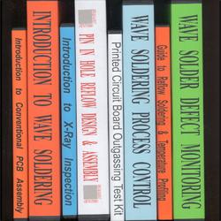
Bob Willis has an extensive range of training videos available online. The complete video collection is available to view online for a fixed fee, based on a six month period. After purchase you are provided with links to each of the online videos for
Electronics Forum | Wed Feb 20 09:05:38 EST 2008 | tonyamenson
We had a similar problem with lead-free through-hole components. We baked those baords to remove the residual moisture and everything went to 100% pass - defect was gone. Couldnt hurt to try a sample run while you decide if the PCB holes need to be
Electronics Forum | Fri Mar 02 08:52:20 EST 2001 | markkrmp
Are your voids looking like blow holes also? Is this only occurring on the solder joints of the Thru Hole components and Via's? Or does this happen on SMD pads? My experience is that we have seen this but only with some of our older PCB's which are
Industry News | 2016-06-27 14:59:09.0
GPD Global introduces the NEW TempView Thermal Imaging System that ensures the success of heated dispensing processes like Underfill, Encapsulations, Dam and Fill, and more. The TempView Thermal Imaging System monitors the temperature of the entire substrate for complete heat profile characterization. Regions of the product may be selected for monitoring during the heating process. Now you can accurately monitor temperature of specific devices to be sure they are up to temperature before starting a process.
Industry News | 2017-04-11 21:19:32.0
GPD Global offers versatile large format inline dispensing systems and stand-alone liquid dispense technologies for maximizing product yield. This is the largest standard PCB dispensing system platform in the industry.
.jpg)
Parts & Supplies | SMT Equipment
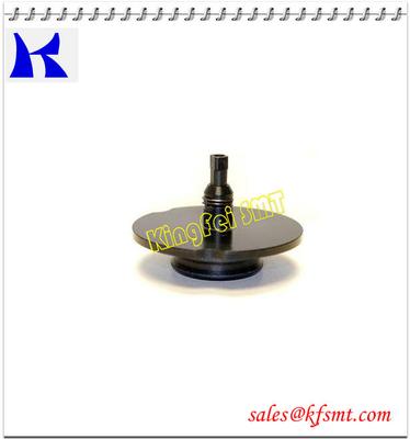
Panasonic smt nozzles models: Panasonic MSR SMT NOZZLE Part Number Description 10468S0002 MSR - SMT NOZZLE - VVS (0.84 X 0.60) 10468S0003 - NZ. - VS (1.0 X 0.64) 10468S0004 -NZ. - S (1.6 X 1.06) 1046710134 -NZ. - M (1.60mm) 10467S0001 -NZ. - L
Parts & Supplies | SMT Equipment
Panasonic smt nozzles models: Panasonic MSR SMT NOZZLE Part Number Description 10468S0002 MSR - SMT NOZZLE - VVS (0.84 X 0.60) 10468S0003 - NZ. - VS (1.0 X 0.64) 10468S0004 -NZ. - S (1.6 X 1.06) 1046710134 -NZ. - M (1.60mm) 10467S0001 -NZ. - L
Technical Library | 2017-11-08 23:22:04.0
Due to the ongoing trend towards miniaturization of power components, the need for increased thermal conductivity of solder joints in SMT processes gains more and more importance. Therefore, the role of void free solder joints in power electronics becomes more central. Voids developed during soldering reduce the actual thermal transfer and can cause thermal damage of the power components up to their failure. For this reason, the company has developed a new technique to minimize the formation of these voids during the soldering process.
Technical Library | 2018-09-21 10:12:53.0
Moisture accumulates during storage and industry practice recommends specific levels of baking to avoid delamination. This paper will discuss the use of capacitance measurements to follow the absorption and desorption behaviour of moisture. The PCB design used in this work, focused on the issue of baking out moisture trapped between copper planes. The PCB was designed with different densities of plated through holes and drilled holes in external copper planes, with capacitance sensors located on the inner layers. For trapped volumes between copper planes, the distance between holes proved to be critical in affecting the desorption rate. For fully saturated PCBs, the desorption time at elevated temperatures was observed to be in the order of hundreds of hours. Finite difference diffusion modelling was carried out for moisture desorption behaviour for plated through holes and drilled holes in copper planes. A meshed copper plane was also modelled evaluating its effectiveness for assisting moisture removal and decreasing bake times. Results also showed, that in certain circumstances, regions of the PCB under copper planes initially increase in moisture during baking.

ACI Technologies Inc. (ACI) is a scientific research corporation dedicated to the advancement of electronics manufacturing processes and materials for The Department of Defense and industry. This video provides an overview of our commercial service
This video describes the IPC A-600 training and certification program. The IPC A-600 specification is a set of acceptability specifications for printed circuit boards. These standards determine the acceptance and reject criteria for printed wiring bo
Training Courses | | | PCB Assembly Courses
The PCB assembly courses provide knowledge of different processes and equipment used in TH and SMT assembly of printed circuit boards.
Training Courses | | | IPC-600 Specialist (CIS)
The Certified IPC-600 Specialist (CIS) training targets quality assurance and acceptance of bare printed circuit boards.
SMTnet Express, December 16, 2017, Subscribers: 31,015, Companies: 10,789, Users: 24,054 Controlling Voiding Mechanisms in the Reflow Soldering Process Keith Sweatman, Takatoshi Nishimura, Kenichiro Sugimoto, Akira Kita; Nihon Superior Co., Ltd
SMTnet Express, April 7, 2022, Subscribers: 25,732, Companies: 11,564, Users: 27,174 Effect Of Vacuum Reflow On Solder Joint Voiding In Bumped Components Voids affect the thermal characteristics and mechanical properties of a
PCB Libraries, Inc. | https://www.pcblibraries.com/Forum/making-mounting-holes-in-footprint_topic1411.html
Making Mounting Holes in Footprint - PCB Libraries Forum Forum Home > PCB Footprint Expert > Questions & Answers New Posts FAQ Search Events Register Login Making Mounting Holes in Footprint
Heller Industries Inc. | https://hellerindustries.com/voids/
Circuit Board Voids Home » Circuit Board Voids Re-printed in partnership with ITM Circuit Board Voids Circuit Board Voids are cavities or air pockets inside the solder joint formed by gases that are released during reflow or by flux residues that fail to escape from the solder

Products, services, training & consulting for the assembly, rework & repair of electronic assemblies. BGA process experts. Manufacturers Rep, Distributor & Service Provider for Seamark/Zhuomao and Shuttle Star BGA Rework Stations.
Training Provider / Manufacturer's Representative / Equipment Dealer / Broker / Auctions / Consultant / Service Provider
1750 Mitchell Ave.
Oroville, CA USA
Phone: (888) 406-2830


.jpg)