Industry Directory | Manufacturer
Photo Stencil provides high-performance stencils, squeegee blades, thick film and metal mask screens and tooling for the surface mount technology (SMT) assembly, solar, and semiconductor industries.
Industry Directory | Manufacturer
Electroform, laser cut, and chem-etch stencils, precision chem-etch metal parts, inspection templates, mesh printing screens. IN BUSINESS OVER 30 YEARS!

Manufacturer: ChuangWei Condition: NEW. It is a stand alone router machine specially designed to route (depanelize) printed circuit board assemblies (PCBA) into individual assemblies. The machine can accomodate larger PCBs in its two table configur

Why select ChuangWei as your depaneling vendor? 1. More choices of machines for scored or routed boards 2. More factory support after purchase 3. Quick turnaround on blade re-sharpening 4. Engineered solutions to challenging applications Fea
Electronics Forum | Fri Jun 10 08:08:54 EDT 2005 | ajaydoshi
thanks a lot for info. If you have some photo, pl. send at ajay_doshi@utlindia.com Photo will help to understand better ajay
Electronics Forum | Fri Oct 03 07:49:18 EDT 2003 | mk
Mask Musings. Soldermask (SM) and its functions have changed and evolved over the years. As an ex-solder mask applicator, I can remember screening Colonial High Gloss Epoxy soldermask on boards back in the early 80's, ending up with a thickness that
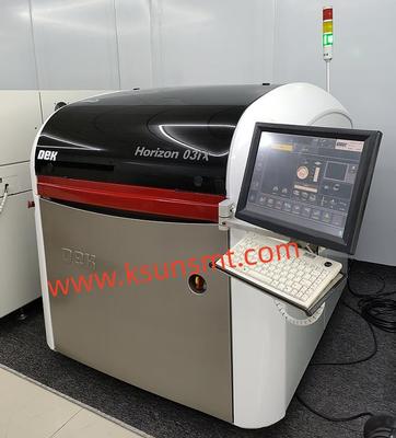
Used SMT Equipment | Screen Printers
DEK Horizon 03iX Fully Automatic Screen Solder Paste Printer Model Horizon 03iX Operating System Win XP+09sp13 or up PCB support Tooling&n
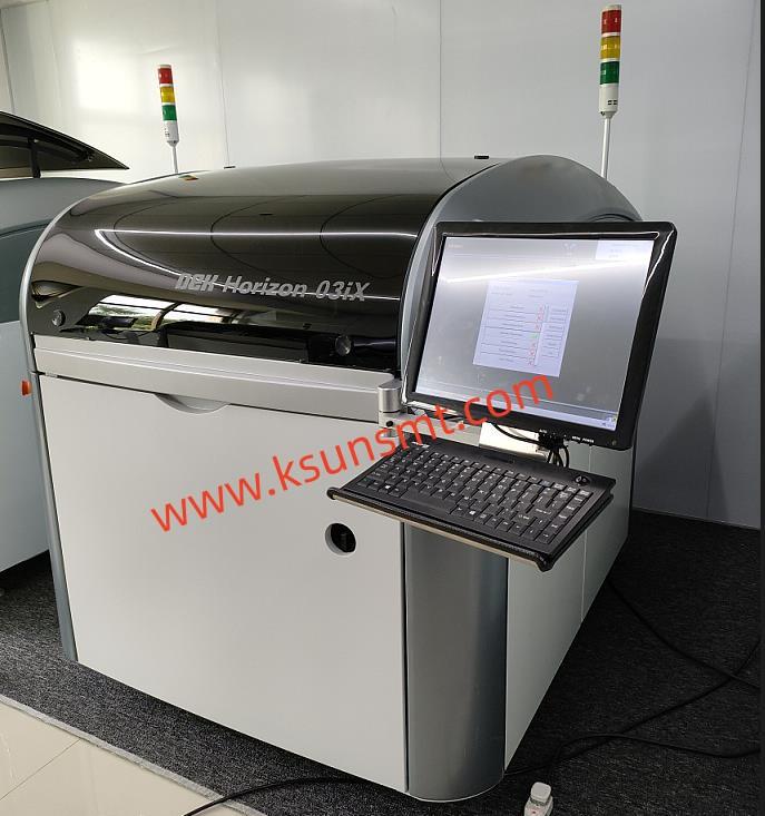
Used SMT Equipment | Screen Printers
DEK Horizon 03iX SMT Printer Model Horizon 03iX Operating System Win XP+09sp13 or up PCB support Tooling Magnetic tooling pins Camera type Hawkeye 750 or Hawkeye 1700 (optional) 198040 198043 hawkeye Board foil clamp siz
Industry News | 2003-03-21 08:12:24.0
Tecan reckons it is consistently producing what may be regarded as the most efficient stencils in the world today.
Industry News | 2003-05-01 09:12:52.0
Press-fit panel-mount light pipes can protect circuits from accidental ESD by isolating the PCB from human contact.
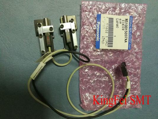
Parts & Supplies | General Purpose Equipment
Thickness Sensor N510015037AA SMT Spare Parts CM212 Photo Sensor SMT Parts

Thickness Sensor N510015037AA SMT Spare Parts CM212 Photo Sensor SMT Parts Part Name: Thickness Sensor Part Number: N510015037AA Application: CM602 CM212 Machine Condition: Original New Country: Japan Brand: Panasonic Model: LV-S72T SO(27
Technical Library | 2024-05-31 19:29:59.0
A-Laser enters the aerospace world with laser cutting services that continue to exceed performance expectations. The modern aerospace industry has strict tolerance requirements and A-Laser is prepared to meet those needs. For example, modern aerospace design dictates anywhere from dozens to millions of precise holes and channels. These must vary in thickness, diameters, and geometries. A-Laser is prepared to meet these requirements and we do so with faster, more versatile, more consistent and cost-effective tools.
Technical Library | 2023-07-25 16:25:56.0
This paper address two significant applications of stencils in advance packaging field: 1. Ultra-Thin stencils for miniature component (0201m) assembly; 2. Deep Cavity stencils for embedded (open cavity) packaging. As the world of electronics continues to evolve with focus on smaller, lighter, faster, and feature-enhanced high- performing electronic products, so are the requirement for complex stencils to assemble such components. These stencil thicknesses start from less than 25um with apertures as small as 60um (or less). Step stencils are used when varying stencil thicknesses are required to print into cavities or on elevated surfaces or to provide relief for certain features on a board. In the early days of SMT assembly, step stencils were used to reduce the stencil thickness for 25 mil pitch leaded device apertures. Thick metal stencils that have both relief-etch pockets and reservoir step pockets are very useful for paste reservoir printing. Electroform Step-Up Stencils for ceramic BGA's and RF Shields are a good solution to achieve additional solder paste height on the pads of these components as well as providing exceptional paste transfer for smaller components like uBGAs and 0201s. As the components are getting smaller, for example 0201m, or as the available real estate for component placement on a board is getting smaller – finer is the aperture size and the pitch on the stencils. Aggressive distances from step wall to aperture are also required. Ultra-thin stencils with thicknesses in the order of 15um-40um with steps of 15um are used to obtain desired print volumes. Stencils with thickness to this order can be potential tools even to print for RDLs in the package.
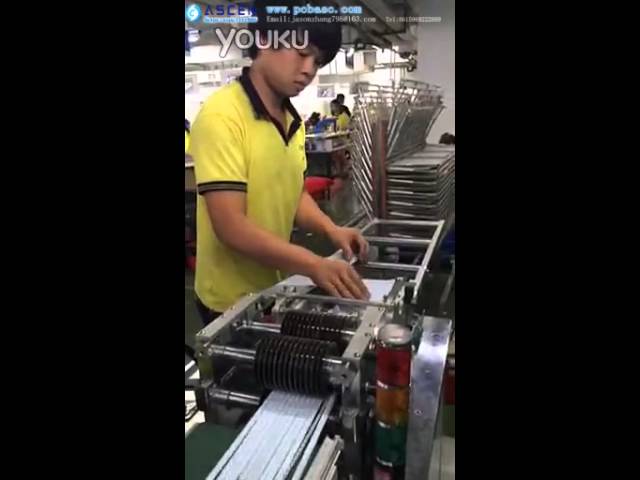
http://www.pcbasc.com/a/PCB_cutter/ http://ascen.en.gongchang.com/ V-cut separator cutting PCB tool pcb depaneling machine auto PCB depanelizer connect smt production line

Singulate Straight Tab Routed Panels Store cut tabs inside tool for discarding at operator convenience Available with 3 blade types and choice of support dies Clean cut - requires no rework for deburring PCB edges Easy blade change in under 5 m
Training Courses | | | IPC-600 Specialist (CIS)
The Certified IPC-600 Specialist (CIS) training targets quality assurance and acceptance of bare printed circuit boards.
Training Courses | | | IPC-600 Trainer (CIT)
The Certified IPC-600 Trainer (CIT) courses recognize individuals as qualified trainers in the area of quality assurance of bare printed circuit boards and prepare them to deliver Certified IPC-600 (CIS) training.
Events Calendar | Wed Apr 19 00:00:00 EDT 2017 - Fri Apr 21 00:00:00 EDT 2017 | Nara, Japan
Ceramic Interconnect and Ceramic Microsystems Technologies (CICMT 2017)
International Microelectronics Assembly and Packaging Society (IMAPS)
Career Center | Chesterland, Ohio USA | Production
Surface Grinder/Lapper Operator Position Overview We currently have an excellent career opportunity for a Surface Grinder/Lapper Operator to join our Ceramics team at our Channel Products, Inc. facility in Chesterland, OH. This position is respons
Career Center | Colorado Springs, Colorado USA | Sales/Marketing
Active customer service support for existing accounts to include both phone and email contact. Coordinate and assist with resolution of locally initialed customer concerns, complaints and corrective actions. Maintain accurate and complete territory a
Career Center | Fort Mill, South Carolina USA | Engineering,Maintenance,Research and Development
Have serviced AMF pinspotters both mechanical and electrical sides; included repair of chassis pc boards to component level. 20 years in this field. Have worked in PCB manufacture with old style board populators and Panasert robots Worked in H
Career Center | Erode, Tamilnadu India | Engineering
Professional Summary 3+ years of experience in the PCB CAM engineering Exposure to FRONTLINE GENESIS 2000 Having exposure in UCAM Exposure to Create, Array & Panelize it for manufacturability Experienced in Creating impedance cou
SMTnet Express, October 16, 2014, Subscribers: 23409, Members: Companies: 14079, Users: 36964 Oxide Thickness and Solderability Methodology to Determine Long Term Storage of BGAs and QFPs. Rama Hegde, senior member of technical staff; Freescale
PCB Libraries, Inc. | https://www.pcblibraries.com/Forum/silkscreen-thickness_topic2280.html
SilkScreen Thickness - PCB Libraries Forum Forum Home > PCB Footprint Expert > Questions & Answers New Posts FAQ Search Events Register Login SilkScreen Thickness
ASYMTEK Products | Nordson Electronics Solutions | https://www.nordson.com/en/divisions/polymer-processing-systems/news/news/2018-10-16-2
Online analytical tool calculates return on investment for advanced Sheet Die designed for fast changes in thickness Polymer Processing Systems


