Henkel offers innovative capillary flow underfill encapsulants for flip-chip, CSP and BGA devices. These are highly flowable, high purity, onecomponent encapsulants. They form a uniform and void-free underfill layer to improve reliability performance
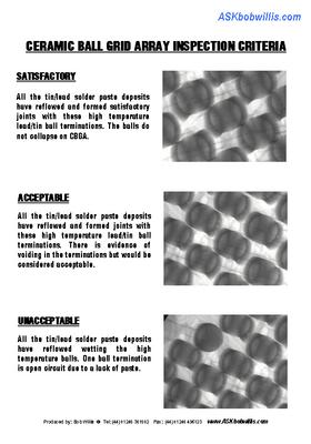
Ball Grid Array X-Ray Inspection Guide - 20 Colour Charts Includes X-Ray inspection guide of satisfactory BGA solder joints and process defects, x-ray images are black and white. The posters are provided as a pdf file and can be printed as A4 or A3
Electronics Forum | Thu Nov 01 10:57:34 EDT 2012 | kris1128
Has anyone heard whether the elevation of a plant can effect solder joint formation? One plant at sea level, one at 7,000 feet elevation... same equipment and profiles, big voiding defects at higher elevation. I did a search and found no similar post
Electronics Forum | Wed May 20 17:18:09 EDT 2009 | daxman
Just out of curiosity, how are you or anyone else determining a defect? Last I checked, IPC had no criteria yet for solder defects for QFN components. Has this changed? Biggest problems we see are voids which our x-ray shows a lot of. Our problems
Industry News | 2015-05-07 19:28:29.0
MIRTEC announce a new strategic cooperation that will empower yield improvement in the electronics manufacturing industry.
Industry News | 2017-05-15 16:35:00.0
SMTA China announces that it presented awards for seven papers and two exhibits at the SMTA China East Conference 2017 Award Presentation Ceremony, held on Tuesday, April 25, 2017 at the Shanghai World Expo Exhibition & Convention Center in conjunction with the SMTA China Annual Award Ceremony.
Technical Library | 2013-01-24 19:16:35.0
The electronics industry has mainly adopted the higher melting point Sn3Ag0.5Cu solder alloys for lead-free reflow soldering applications. For applications where temperature sensitive components and boards are used this has created a need to develop low melting point lead-free alloy solder pastes. Tin-bismuth and tin-bismuth-silver containing alloys were used to address the temperature issue with development done on Sn58Bi, Sn57.6Bi0.4Ag, Sn57Bi1Ag lead-free solder alloy pastes. Investigations included paste printing studies, reflow and wetting analysis on different substrates and board surface finishes and head-in-pillow paste performance in addition to paste-in-hole reflow tests. Voiding was also investigated on tin-bismuth and tin-bismuth-silver versus Sn3Ag0.5Cu soldered QFN/MLF/BTC components. Mechanical bond strength testing was also done comparing Sn58Bi, Sn37Pb and Sn3Ag0.5Cu soldered components. The results of the work are reported.
Technical Library | 2012-10-18 21:58:51.0
First published in the 2012 IPC APEX EXPO technical conference proceedings. In this paper, we report on a comprehensive study regarding the morphology evolution and voiding of SnAgCu solder joints on the central pad of two different packages – QFN and an Agilent package called TOPS – on PCBs with a Ni/Au surface finish.

This video describes the IPC A-600 training and certification program. The IPC A-600 specification is a set of acceptability specifications for printed circuit boards. These standards determine the acceptance and reject criteria for printed wiring bo
Training Courses | ON DEMAND | | IPC-600 Trainer (CIT)
The Certified IPC-600 Trainer (CIT) courses recognize individuals as qualified trainers in the area of quality assurance of bare printed circuit boards and prepare them to deliver Certified IPC-600 (CIS) training.
Events Calendar | Thu Oct 03 00:00:00 EDT 2019 - Thu Oct 03 00:00:00 EDT 2019 | ,
IPC Tech Ed Webinar Series: Ball Grid Array (BGA) and Bottom Termination Component (BTC) Design and Assembly Challenges: Reflow Profiling to Achieve Low Defect Rates and Successful Assembly! – Part 2
Events Calendar | Tue Feb 12 00:00:00 EST 2019 - Tue Feb 12 00:00:00 EST 2019 | ,
Webinar: BGA and Area Array Process Defects - Causes & Cures
Minimizing Voiding In QFN Packages Using Solder Preforms SMTnet Express July 27, 2012, Subscribers: 25333, Members: Companies: 8933, Users: 33366 Minimizing Voiding In QFN Packages Using Solder Preforms First published in the 2012 IPC APEX EXPO
The Morphology Evolution and Voiding of Solder Joints on QFN Central Pads with a Ni/Au Finish SMTnet Express October 19, 2012, Subscribers: 25598, Members: Companies: 9011, Users: 33828 The Morphology Evolution and Voiding of Solder Joints on QFN