Industry Directory | Manufacturer
Shuttle Star Technology designs and builds advanced off-line 2.5D&3D x-ray inspection systems for solder joint and final assembly test inspection in SMT&EMS. It uses world-class X-ray techniques with advanced defect detection.
In-Line X-ray Inspection System Automatically in-line inspect Solder joint defects of PCBA and other defects on Hidden Components. Able to judge Good/NG fast with inspection speed of 1sec/FOV and the program can set ROIs conveniently. Performing X-r
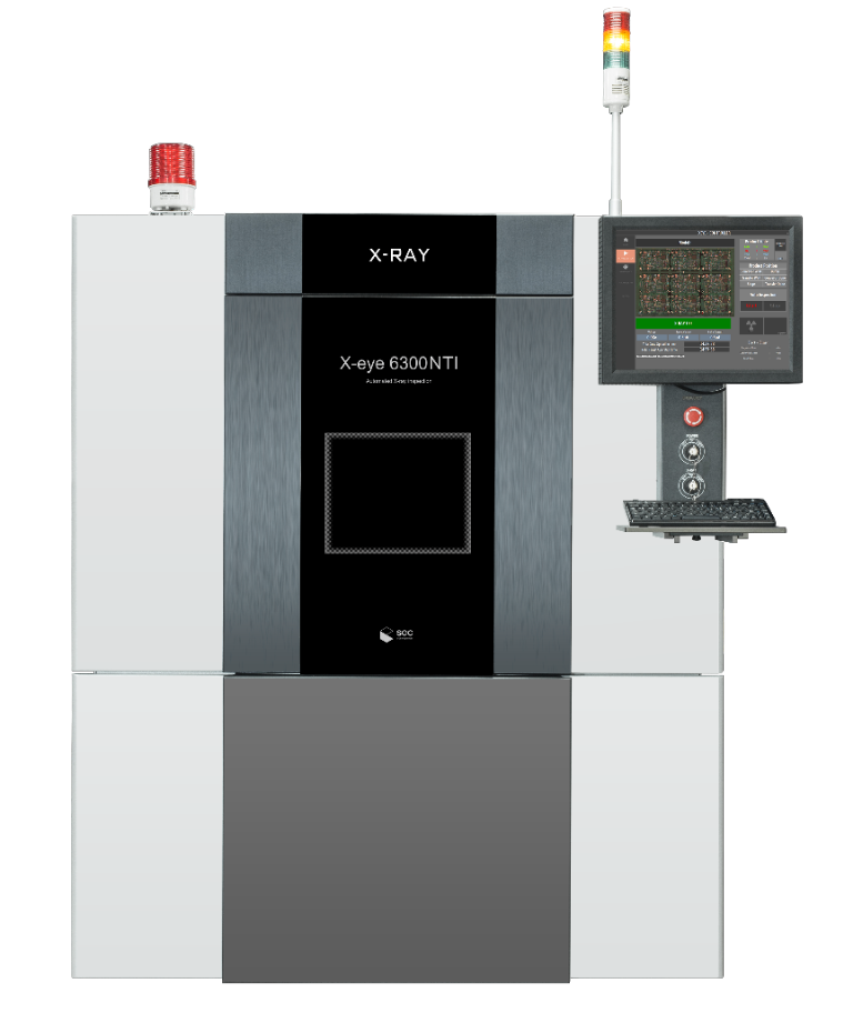
In-Line X-ray Inspection System Automatically in-line inspect Solder joint defects of PCBA and other defects on Hidden Components. Able to judge Good/NG fast with inspection speed of 1sec/FOV and the program can set ROIs conveniently. Performing X-r
Electronics Forum | Thu Mar 25 09:38:36 EDT 2021 | spoiltforchoice
Well everything Graham said with some additional points.. You mention manual printing but very little about your stencil or setup. Everything you have said indicates a very limited budget has been expended, however what you have is an extreme exampl
Electronics Forum | Mon Sep 23 01:28:13 EDT 2019 | sssamw
Cannot understood your problem very clearly, please check IPC standard on QFN and its mfg process, also check the QFN supplier's recommendation, so can minimize the bridge.
Industry News | 2017-04-24 19:04:48.0
This year, MIRTEC will launch several new inspection machines equipped new cutting-edge technologies. MIRTEC is proud to be promoting these new machines in booth #1J10 at NEPCON China 2017, one of the biggest technical exhibitions of SMT and EMA, from April 25-27 at the Shanghai World EXPO Exhibition & Convention Center. MIRTEC’s new machines have been developed under a concept, ‘Perfect Inspection Solution’. This is an inspection concept involving the combination of 3D, 2D, and side-camera inspection.
Industry News | 2014-09-19 20:19:38.0
KYZEN is pleased to announce that Dr. Mike Bixenman will present the paper titled “QFN Design Considerations to Improve Cleaning – A Follow on Study” at the upcoming SMTA International exhibition.
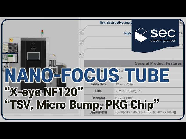
#Xray#Inspection#SEC Nano-focus Tube of 200 nano resolution which is specialized for sub-micron defects of Semiconductor Packaging, Wafer Level Packaging(WLP). -Non-destructive Analysis System -High-Resolution Image with Dual Type CTs -Application
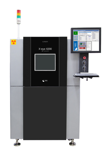
Semi-automated, programmable X-ray inspection system with multi-axis for prototyping, failure analysis, manufacturing process validation and rework verification for PCBs up to 18 x 20". The XT-3 is a high quality high-resolution manual x-ray inspecti
Defect Free QFN Assembly Defect Free QFN Assembly The problem with soldering QFN packages is that they float, skew and tilt on the 'domed' melted solder during the SMT re-flow process. This floating, skewing and/or tilting will lead to solder


