Industry Directory | Consultant / Service Provider / Manufacturer
Specializing in electronic circuit board assembly services. Various capabilities include engineering, assembly, designing, prototyping,supply chain management, testing, documentation, rework, repair and soldering. On-time delivery
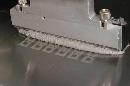
New Equipment | Solder Materials
Indium Corporation manufactures high quality solder powders and pastes. Powders are available in hundreds of alloys and a full range of sizes. Solder pastes can be made from these powders using a wide variety of flux vehicles to get the best fit for
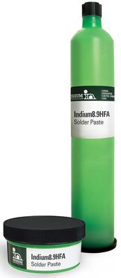
New Equipment | Solder Materials
Solves: QFN Voiding | Head-in-Pillow | Graping Indium8.9 is an air or nitrogen reflow, no-clean solder paste specifically formulated to accommodate the higher processing temperatures required by the SnAgCu, SnAg, and other alloy systems favored by t
Electronics Forum | Thu Mar 16 03:45:51 EDT 2017 | rob
It's the same thermal issue whether it's a die or package. It's different if it is just a signal trace, but if it's a heatsink pad (LED, FET, Motor driver, PSU IC etc). I think the voiding issue boils down to what the part is actually doing. The or
Electronics Forum | Wed Mar 15 12:39:24 EDT 2017 | cyber_wolf
Customer precedes standard, but customer must be educated and informed on what is achievable with their design and what is accepted as industry standard practice. My guess is that the negative effect of those voids is negligible. {Voids at the sold
Industry News | 2003-06-10 08:16:44.0
The following text describes the application of NWA Quality Analyst to quality control in the assembly of electronic components.
Industry News | 2016-01-17 19:26:58.0
In order to keep up with industry demand, IPC has released amendments for J-STD-001F, Requirements for Soldered Electrical and Electronic Assemblies, and IPC-A-610F, Acceptability of Electronic Assemblies. For each standard, IPC-A-610F Amendment 1 and IPC J-STD-001F Amendment 1 represents a critical shift to deliver necessary updates to these already robust standards.
Technical Library | 2023-08-04 15:38:36.0
The MicroLeadFrame® (MLF®)/Quad Flat No-Lead (QFN) packaging solution is extremely popular in the semiconductor industry. It is used in applications ranging from consumer electronics and communications to those requiring high reliability performance, such as the automotive industry. The wide acceptance of this packaging design is primarily due to its flexible form factors, size, scalability and thermal dissipation capabilities. The adaptation and acceptance of MLF/QFN packages in automotive high reliability applications has led to the development of materials and processes that have extended its capabilities to meet the performance and quality requirements. One of process developments that is enabling the success of the MLF/QFN within the automotive industry has been the innovation of side wettable flanks that provide the capability to inspect the package lead to printed circuit board (PCB) interfaces for reliable solder joints. Traditionally, through-board X-ray was the accepted method for detecting reliable solder joints for leadless packages. However, as PBC layer counts and routing complexities have increased, this method to detect well-formed solder fillets has proven ineffective and incapable of meeting the inspection requirements. To support increased reliability and more accurate inspection of the leadless package solder joints, processes to form side-wettable flanks have been developed. These processes enable the formation of solder fillets that are detectable using state-of-the-art automated optical inspection (AOI) equipment, providing increased throughput for the surface mount technology (SMT) processes and improved quality as well.
Technical Library | 2020-11-24 23:01:04.0
The miniaturization trend is driving industry to adopting low standoff components or components in cavity. The cost reduction pressure is pushing telecommunication industry to combine assembly of components and electromagnetic shield in one single reflow process. As a result, the flux outgassing/drying is getting very difficult for devices due to poor venting channel. This resulted in insufficiently dried/burnt-off flux residue. For a properly formulated flux, the remaining flux activity posed no issue in a dried flux residue for no-clean process. However, when venting channel is blocked, not only solvents remain, but also activators could not be burnt off. The presence of solvents allows mobility of active ingredients and the associated corrosion, thus poses a major threat to the reliability. In this work, a new halogen-free no-clean SnAgCu solder paste, 33-76-1, has been developed. This solder paste exhibited SIR value above the IPC spec 100 MΩ without any dendrite formation, even with a wet flux residue on the comb pattern. The wet flux residue was caused by covering the comb pattern with 10 mm × 10 mm glass slide during reflow and SIR testing in order to mimic the poorly vented low standoff components. The paste 33-76-1 also showed very good SMT assembly performance, including voiding of QFN and HIP resistance. The wetting ability of paste 33-76-1 was very good under nitrogen. For air reflow, 33-76-1 still matched paste C which is widely accepted by industry for air reflow process. The above good performance on both non-corrosivity with wet flux residue and robust SMT process can only be accomplished through a breakthrough in flux technology.
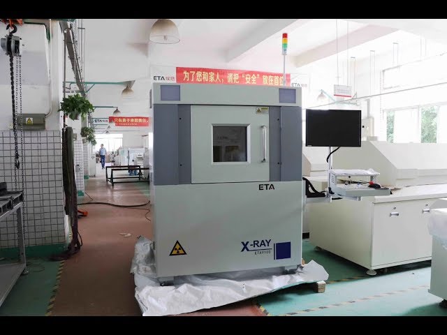
SMT PCBA X-ray Machine ETA-7900 If you could not find any similar items you want, you may send some photos to us. because our catalog and website haven't included all of our products. smt x ray,smt x ray machine,x-ray inspection machine,x-ray d

In this video we show you how to perform an automated x-ray inspection using the TruView Prime
The Morphology Evolution and Voiding of Solder Joints on QFN Central Pads with a Ni/Au Finish SMTnet Express October 19, 2012, Subscribers: 25598, Members: Companies: 9011, Users: 33828 The Morphology Evolution and Voiding of Solder Joints on QFN
SMTnet Express, August 8, 2019, Subscribers: 32,214, Companies: 10,853, Users: 25,321 Novel Approach to Void Reduction Using Microflux Coated Solder Preforms for QFN/BTC Packages that Generate Heat Credits: Alpha Assembly Solutions The requirement
ASYMTEK Products | Nordson Electronics Solutions | https://www.nordson.com/en/divisions/dage/application/smt
. For applications where the QFN may be subjected to regular shocks (for example in a mobile phone) mechanical pull and shear testing ensures adhesion strength is acceptable and protects against future latent failures. More information
PCB Libraries, Inc. | https://www.pcblibraries.com/Forum/topic2593&OB=DESC.html
. The smallest visible markings range from 0.30 mm – 0.40 mm and are typically used for micro-miniature packages or very dense part placement PCB layouts


.gif)
