Industry Directory | Distributor
UniversityWafer is a leading silicon wafer and semiconductor substrate supplier to for academia and industry. We provide high-quality, low cost wafers in small and large quantities. Why buy wafers in volume when you don't to!
Industry Directory | Manufacturer
Full service supplier of silicon wafers and wafer processing services, including polishing, reclaim, thermal oxide and back-grinding. Supplies silicon wafers in all specifications from 2in. to 300mm in diameter.
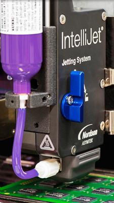
The IntelliJet® Jetting System with patented ReadiSet™ Jet Cartridge delivers cutting-edge reliability and micro dot dispensing for manufacturing advanced semiconductor and mobile electronics packages The piezo-driven IntelliJet system is the world'
Full service supplier of silicon wafers and wafer processing services, including polishing, reclaim, thermal oxide and back-grinding. Supplies silicon wafers in all specifications from 2in. to 300mm in diameter.
Electronics Forum | Tue Feb 02 09:51:38 EST 1999 | Justin Medernach
| Hello Everybody: | | I am in urgent need of some information regarding the reflow profile for a flip chip wafer. Would the reflow conditions along with the flux used affect the appearence of the solder joints. | | We are witnessing dull solder j
Electronics Forum | Tue Jan 16 20:34:17 EST 2007 | davef
DAVE�S BOOKSHELF ASSEMBLER�S ESSENTIALS Title: Soldering in ElectronicsAuthor: RJ Klein WassinkPublisher: Electrochemical PublicationsISBN: 090115024XPublication date: December 1989 I know, I know. The book was written in 1989!!!! I use this b
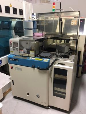
Used SMT Equipment | Semiconductor & Solar
· Dual Magnification, auto-focusing Optical System · DC brushless, 60,000 RPM closed-loop speed-controlled Air Bearing Spindle · Front loaded dual Cassette Compartment · Inspection Drawer - also used for single wafer load/unload · Dress Wafe
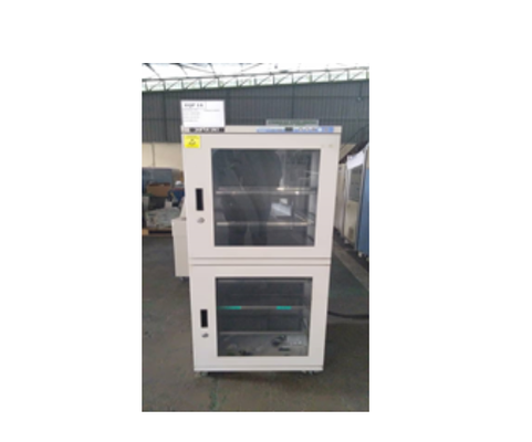
Used SMT Equipment | Drying Equipment
BRAND : SUPER DRY -02 SERIES MODEL : SD-3032-02 DESCRIPTIONS : "02 series are equipped with 1 patented dry unit to constantly main
Industry News | 2018-12-08 03:20:37.0
Top Silicon Wafer Manufacturing Companies in the World
Industry News | 2014-04-15 08:53:30.0
— ISVI Corporation will exhibit at The Vision Show, scheduled to take place April 15-17, 2014 at the Hynes Convention Center in Boston, MA.
 EJECTOR 40010678 CVX-0611,MPS V6C-AC-JU(1)1.jpg)
Parts & Supplies | Pick and Place/Feeders
Supply & repair juki ejector at a lower price: JUKI 750(760) EJECTOR E79117250A0 VP*0749 JUKI 750(760) EJECTOR (E3066700000,PISCO VBH07-46) JUKI 750(760) 4-WAY ELECTROMAGNETIC VALVE PV140507000 VQD1121W-5MO-C4-X8B JUKI 750(760) ELECTROMAGNETIC V
Parts & Supplies | Pick and Place/Feeders
JUKI 40019547 CONVEYOR EXTENSION BELT 250 FUJINTAI TECHNOLOGY CO.,LTD JUKI 40019838 MONITOR CABLE ASM www.fujintai.com JUKI 40019928 "GEAR,SPROCKET(MOD)" FUJINTAI TECHNOLOGY CO.,LTD JUKI 40019929 MOTOR 24VDC www.fujintai.com JUKI 40020166 CONVEYO
Technical Library | 1999-08-05 10:45:36.0
In 1998, the International 300 mm Initiative (I300I) demonstration and characterization programs will focus on 180 nm technology capability. To support these activities, I300I and equipment supplier demonstration partners must use starting silicon wafers with key parameters specified at a level appropriate level for 180 nm processing, including contamination and lithographic patterning. This document describes I300I's silicon wafer specifications, as developed with the I300I Silicon Working Group (member company technical advisors) and SEMI Standards.
Technical Library | 2009-05-28 18:15:46.0
Considerable effort is ongoing to improve the efficiency and to move towards high-volume manufacturing of photovoltaic cells. Much attention has been focused on developing in-line processes to replace the current batch processes. A critical process to improve the performance of solar wafers is the application of Dopants. The basic requirement for this process is an automated method for applying a very thin, uniform film of Dopant to the silicon wafer as part of an in-line manufacturing process.
Why you should attend International Wafer-Level Packaging Conference, October 23 - 25, 2018 in San Jose, California, USA.

This is the first in a series of 10-minute videos to introduce new users to the basics of machine vision technology. In this video, users will learn what machine vision is, how it is used in factory automation, and its four most common applications.
Training Courses | | | PCB Design Courses
The PCB design courses teach students the process, techniques and tools needed to design layout of printed circuit boards.
Events Calendar | Tue Feb 15 00:00:00 EST 2022 - Thu Feb 17 00:00:00 EST 2022 | San Jose, California USA
Wafer-Level Packaging Symposium
Events Calendar | Wed Feb 14 00:00:00 EST 2024 - Fri Feb 16 00:00:00 EST 2024 | San Francisco, California USA
Wafer-Level Packaging Symposium
Career Center | Charlton, Massachusetts USA | Engineering,Management,Production,Research and Development
MANUFACTURING / PROCESS ENGINEER Fused Fiber Optics company is seeking a Process Engineer to support its Optical Fabrication department. This position will be responsible for process development, optimization and troubleshooting, as well as the prep
Career Center | NORTHRIDGE, California USA | Engineering
EDUCATION BS Electronics and Communication Engineering Gujarat University MS Electrical Engineering California State University, Northridge ACADAMIC PROJECT Fabrication and Characterization of Silicon Carbide (SiC) MESFE
Career Center | Melbourne, Florida USA | Management,Production,Quality Control
Technical Skills/Abilities: � Management � Quality Assurance � Strong Troubleshooting Skills � Strategic Planning � Employee Training � Quality Assurance � Problem Resolution � Mechanical/Technical Aptitude
Wafer-Level Packaged MEMS Switch With TSV Wafer-Level Packaged MEMS Switch With TSV by: Nicolas Lietaer, Thor Bakke, Anand Summanwar; SINTEF , Per Dalsjø, Jakob Gakkestad; Norwegian Defence Research Establishment (FFI), Frank Niklaus; KTH - Royal


winsouce.jpg)