New Equipment | Solder Materials
Big-Size Vacuum Soldering Oven for IGBT, MOS 1.Reflow soldering Typically high number of voids cause a large non conductive area 2.Vacuum soldering Very low number of voids, Typically 3.Applications Power Semiconductors;Hybrid

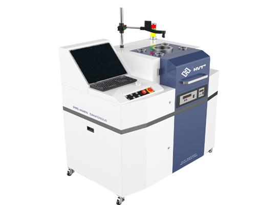
New Equipment | Soldering - Other
Sunny Company:Beijing Chengliankaida Technology Co.,Ltd Address : SanCang Road Sanjianfang airport ,Tongzhou district , Beijing China Email: salemachines@bjclkdkj.cn Skype :smdsupplier Whatsapp: +86 159 01434496 Wechat: + 86 159 0143 4496
Electronics Forum | Sat Sep 23 15:13:40 EDT 2000 | Francois Racine
Hi Sophia, I`m responsible of SMT line and we solved this problem with a complete automatic solder paste printer machine. In the past we had problem with off alignment and solder height too.... at that time we used a semi-auto printer machine and w
Electronics Forum | Fri Nov 26 06:18:18 EST 1999 | stefano bolleri
Jeff & Ted, we have used a dispensing system too and yes, I agree, we are not too happy with the results. Not at the point that it doesn't work, though. I think our problem basicly is that we have selected an entry-level dipensing system. We are app
Industry News | 2007-11-01 20:29:37.0
November 1, 2007 - Lloyd Doyle announces they will showcase the IBIS system, a brand new development for solder bump inspection, in Hall A1 Stand 347 at the upcoming Productronica 2007 exhibition and conference scheduled to take place November 13-16, 2007 at the Munich Trade Fair Center in Munich, Germany.
Industry News | 2003-06-13 10:10:58.0
By combining PacTech's electroless under bump metallization (UBM) processing with DEK's advanced mass imaging systems to create the solder bumps, users can implement a wafer-level, SMT-compatible flip chip assembly process.
Technical Library | 2023-01-17 17:58:36.0
Heterogeneous integration has become an important performance enabler as high-performance computing (HPC) demands continue to rise. The focus to enable heterogeneous integration scaling is to push interconnect density limit with increased bandwidth and improved power efficiency. Many different advanced packaging architectures have been deployed to increase I/O wire / area density for higher data bandwidth requirements, and to enable more effective die disaggregation. Embedded Multi-die Interconnect Bridge (EMIB) technology is an advanced, cost-effective approach to in-package high density interconnect of heterogeneous chips, providing high density I/O, and controlled electrical interconnect paths between multiple dice in a package. In emerging architectures, it is required to scale down the EMIB die bump pitch in order to further increase the die-to-die (D2D) communication bandwidth. Aa a result, bump pitch scaling poses significant challenges in the plated solder bump reflow process, e.g., bump height / coplanarity control, solder wicking control, and bump void control. It's crucial to ensure a high-quality solder bump reflow process to meet the final product reliability requirements. In this paper, a combined formic acid based fluxless and vacuum assisted reflow process is developed for fine pitch plated solder bumping application. A high-volume production (HVM) ready tool has been developed for this process.
Technical Library | 2016-01-12 11:04:35.0
3D packaging has recently become very attractive because it can provide more flexibility in device design and supply chain, reduce the gap between silicon die and organic substrate, help miniaturize devices and meet the demand of high speed, provide more memory, more function and low cost. With the advancement of 3D packaging, the bump height is now down from 80μ to 10μ. When the bump diameter is 20-40μ and height 10μ, the process and reliability are obvious issues. It is well known that underfill can enhance the reliability for regular flip chip, however underfill won’t help assembly process. In order to resolve some difficulties that 3D packaging faces, YINCAE Advanced Materials, LLC has developed solderable anisotropic conductive adhesives for 3D package applications. In this paper we will discuss the assembly process and reliability in detail.
PCB Dynamic Coplanarity At Elevated Temperatures PCB Dynamic Coplanarity At Elevated Temperatures iNEMI's SMTAI 2011 presentation by: John Davignon, Ken Chiavone, Jiahui Pan, James Henzi, David Mendez, Ron Kulterman; Intel Corporation


