Industry Directory | Manufacturer
The exclusive supplier of SIPAD Solid Solder Deposit in North America and the only SIPAD Solid Solder Deposit (SSD) coating service bureau in the world.
New Equipment | Rework & Repair Services
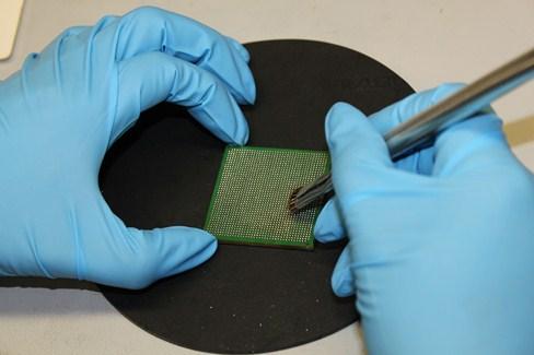
BGA Reballing Services BEST provides BGA reballing services for your plastic-, ceramic- and metalbodied components down to 0.3mm pitch. We have the ability to develop the BGA reballing process you want with a variety of deballing methods and machine
New Equipment | Rework & Repair Services
Your BEST Source For High Quality Industry-Leading BGA Repair Service BEST provides industry-leading solutions for Ball Grid Array BGA Repair Services and other grid array device reworks. Our engineers have developed better processes to make our BGA
Electronics Forum | Mon Aug 09 04:15:33 EDT 1999 | Jacqueline Coia
I am having cleaning problems when processing PCB's which have TAIYO solder mask on them. After processing, hand soldering and cleaning, a sticky residue is remains, resulting in a cosmetically poor finish with tide marks etc. Other soldermasks do no
Electronics Forum | Mon Aug 09 18:03:28 EDT 1999 | Earl Moon
| | I am having cleaning problems when processing PCB's which have | | TAIYO solder mask on them. After processing, hand soldering and | | cleaning, a sticky residue is remains, resulting in a cosmetically poor finish with tide marks etc. Other solde
Industry News | 2023-10-16 12:50:01.0
MIRTEC announces the release of their All-New ART Hybrid 3D AOI System at Productronica 2023. The World's leading trade fair for the electronics manufacturing industry will take place Nov. 14-17, 2023, at the Trade Fair Center Messe München, Germany. All are welcome to MIRTEC's Booth #461 in Hall A2 for a detailed demonstration of what will undoubtedly be recognized as the World's Most Technologically Advanced 3D AOI System!
Industry News | 2012-11-07 11:01:55.0
IPC and SMTA jointly announce the agenda for Session 6 of the High-Reliability Cleaning and Coating Conference, scheduled to take place November 13-15, 2012 at the Crowne Plaza Hotel – O’Hare in Chicago, IL.

Parts & Supplies | Pick and Place/Feeders
The definition of SMT SMT is the surface assembly technology,surface mount technology(surface mount technology)(Surface Mounted Technology abbreviation),is currently the most popular electronic assembly industry,a technology and technology. What a
Technical Library | 2023-01-17 17:19:44.0
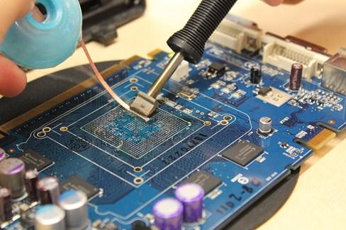
A test program was developed to evaluate the effectiveness of vacuum reflow processing on solder joint voiding and subsequent thermal cycling performance. Area array package test vehicles were assembled using conventional reflow processing and a solder paste that generated substantial void content in the solder joints. Half of the population of test vehicles then were re-processed (reflowed) using vacuum reflow. Transmission x-ray inspection showed a significant reduction in solder voiding after vacuum processing. The solder attachment reliability of the conventional and vacuum reflowed test vehicles was characterized and compared using two different accelerated thermal cycling profiles. The thermal cycling results are discussed in terms of the general impact of voiding on solder thermal fatigue reliability, results from the open literature, and the evolving industry standards for solder voiding. Recommendations are made for further work based on other void reduction methods and additional reliability studies.
Technical Library | 2019-09-19 00:28:48.0
The symbiotic relationship between solder masks and selective finishes is not new. The soldermask application is one of the key considerations to ensure a successful application of a selective finish. The selective finish is the final chemical step of the PCB manufacturing process, this is when the panels are at their most valuable and are unfortunately not re-workable. Imperfections are not tolerated, even if they are wholly cosmetic. Quality issues often manifest themselves in the form of a 'ping pong' conversation between the fabricators, the soldermask suppliers and the selective finish suppliers. Without tangible evidence these discussions are difficult to resolve and the selective finish process is usually regarded as responsible. This paper will focus on the chemical characteristics and use them to predict or identify potential issues before they occur rather than specifically name 'critical' soldermasks. It is also the intention of this paper to address the potential of a soldermask to react to common yield hiking practices like UV bumping and oven curing. It is hoped that this awareness will help fabricators to ensure maximum yields by asking the right questions. 'Critical’ soldermasks impact all selective finishes. In this paper, practical experience using immersion tin will be used to highlight the relationship between 'critical' soldermasks and some of the issues seen in the field. The paper will include a novel approach to identify re-deposited volatiles after the reflow.
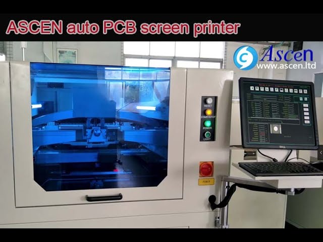
https://www.ascen.ltd/Products/Solder_paste_printer/513.html full auto PCB screen printer and SMT solder paste printing machine with Image and optical system,It is a very accurate fully automatic SMT stencil printer.automatic PCB screen printer main
https://www.ascen.ltd/Products/Solder_paste_printer/513.html full auto PCB screen printer and SMT solder paste printing machine with Image and optical system,It is a very accurate fully automatic SMT stencil printer.automatic PCB screen printer main
Training Courses | | | PCB Assembly Courses
The PCB assembly courses provide knowledge of different processes and equipment used in TH and SMT assembly of printed circuit boards.
Events Calendar | Mon Apr 12 00:00:00 EDT 2021 - Mon Apr 12 00:00:00 EDT 2021 | ,
Europe Chapter Webinar: Tombstoning Components during Reflow Soldering - Causes & Cures
Events Calendar | Wed Jul 13 00:00:00 EDT 2022 - Wed Jul 13 00:00:00 EDT 2022 | Oshkosh, Wisconsin USA
Wisconsin Chapter: PCB Workshop and PCB Plant Tour
Career Center | NORTHRIDGE, California USA | Engineering
EDUCATION BS Electronics and Communication Engineering Gujarat University MS Electrical Engineering California State University, Northridge ACADAMIC PROJECT Fabrication and Characterization of Silicon Carbide (SiC) MESFE
Career Center | , | Engineering,Production,Quality Control
SMT EXPERT WITH DOE ,DFM AND LEAN SKILLS
ATTENDANT WET CHEMICAL PROCESSES) Hole wall preparatio
Non-Contact Streaming Technology Enhances the Dispense Process News Forums SMT Equipment Company Directory Calendar Career Center Advertising About FREE Company Listing! Non-Contact Streaming Technology Enhances the Dispense
Imagineering, Inc. | https://www.pcbnet.com/blog/what-is-solder-mask-color-selecting-the-right-option-for-your-product/
(unintentional connections between two conductors.) After a solder mask is applied, openings must be made by photolithography . Photolithography uses a photosensitive chemical photoresist to transfer geometric patterns onto the wafer
Heller Industries Inc. | https://hellerindustries.com/wp-content/uploads/2020/02/Void-Reduction-Warpage-Vacuum-Reflow-Soldering.pdf
) of the system while still achieving the void rate reduction < 1%. Another key capability that will be explored is the elimination of solder splatter during the process of vacuum purge down


.png)

winsouce.jpg)