Industry Directory | Manufacturer
Reflow ovens for automated SMT PCB assembly, specializing in lead free processing and nitrogen reflow. The best convection reflow ovens on the market.
Industry Directory | Manufacturer
Manufacturers of Automated Optical Inspection

Flux Free Formic Reflow Reflow in Formic Acid Vapor Heller has designed and built an production ready horizontal reflow oven for formic acid vapor. This new oven has been designed to meet Semi S2/S8 safety standards (including toxic gases). Form
New Equipment | Surface Finish
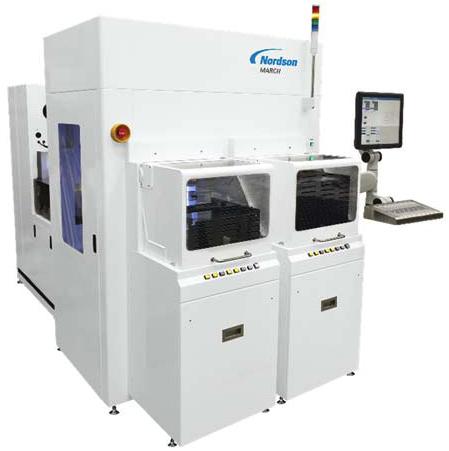
Designed for wafer processing, Nordson MARCH's SPHERE™ series plasma systems, the StratoSPHERE offers superior plasma treatment for high-throughput advanced semiconductor packaging applications. The StratoSPHERE plasma system is ideal for wafer pro
Electronics Forum | Mon Sep 28 12:55:37 EDT 1998 | Manish Ranjan
Hi Everyone Does anyone has any insight regarding the void formation in the solderbumps during wafer bumping by electroplating. Someone told me that it could be mainly coz of the alloy concentration being incorrect. Any suggestions, corrective action
Electronics Forum | Tue Feb 24 01:19:01 EST 1998 | Jon Gruett
You are right !!! The exact volume of solder paste onto flip chips is extremely critical. Only one vendor that I know has taken that part of the process to the next level, whereby they can effectively deposit the right amount onto the flip chip exa
Industry News | 2003-01-27 10:27:31.0
At a New Facility Within the Company's U.S. Headquarters
Industry News | 2018-12-08 03:20:37.0
Top Silicon Wafer Manufacturing Companies in the World
Technical Library | 2020-01-28 00:23:58.0
This paper explores new advances in the reflow soldering process including vacuum technology and warpage mitigation systems. The first topic for discussion will be the implementation of a vacuum process directly in a conventional inline soldering system. The second topic presented is the mitigation of warpage on substrates or wafers.
Technical Library | 2007-12-06 11:37:15.0
Over the past 30 years we have learned that lead has negative affects on the health of humans and seen strong legislation remove it from gasoline and paints. More recently, governments in Europe and Asia have set deadlines to remove lead from consumer electronic devices that use printed circuit boards. Currently, the ban is not being applied to high reliability applications such as military or medical devices, but we all know that will come someday soon. Likewise many believe that lead free solder is coming to wafer bump reflow and are beginning to make the transition.
Nano-copper sintering in formic acid vapor.
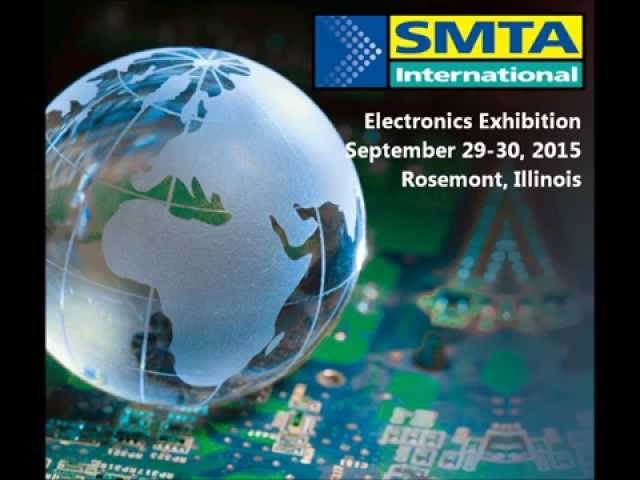
SMTA International Electronics Exhibition Tuesday, September 29: 9am-5pm Wednesday, September 30: 9am-4pm Donald Stephens Convention Center Rosemont, IL See More Equipment & Technology Than Ever Before! Many of the 160 exhibiting companies will bri
Training Courses | | | PCB Design Courses
The PCB design courses teach students the process, techniques and tools needed to design layout of printed circuit boards.
Events Calendar | Sun Sep 27 00:00:00 EDT 2020 - Thu Oct 01 00:00:00 EDT 2020 | Rosemont, Illinois USA
SMTA International 2020 Conference & Exhibition
Events Calendar | Mon Apr 23 00:00:00 EDT 2018 - Thu Apr 26 00:00:00 EDT 2018 | Shanghai, China
SMTA China East Conference 2018
Career Center | Boulder, Colorado USA | Engineering,Production,Quality Control
Senior-level micro-electronic technician capable of independent manufacture of custom hybrids, focal plane assemblies, and prototype detector assemblies in cleanroom environment (in Advanced Packaging and Detector Laboratory). MINIMUM QUALIFICATIONS
Career Center | Sherman, Texas USA | Engineering,Production,Research and Development,Technical Support
SMT Packaging Engineer: Location: Texas - Sherman , TX Group: HVAL Degree Requirements: BS ME/ChemE/Materials The person in this position will have the ability to make very significant financial contributions to TI because this is a very critic
Career Center | NORTHRIDGE, California USA | Engineering
EDUCATION BS Electronics and Communication Engineering Gujarat University MS Electrical Engineering California State University, Northridge ACADAMIC PROJECT Fabrication and Characterization of Silicon Carbide (SiC) MESFE
Career Center | Botevgrad, Sofia Bulgaria | Engineering,Production,Quality Control,Research and Development,Sales/Marketing
AOI - Omron RNS/RNS_ptH, VI3000, Marantz 22X IPC-610D Class 3, Pb/Pb free process, 5S, FMEA, MSA, PPAP, SPC, CPK, 6Sigma, lean manufacturing, Quality management, ISO/TS 16949 ,ISO 9001,ISO 14 001
Reliability Enhancement of Wafer Level Packages with Nano-Column-Like Hollow Solder Ball Structures Reliability Enhancement of Wafer Level Packages with Nano-Column-Like Hollow Solder Ball Structures by: Ronak Varia, Xuejun Fan; Lamar University
Wafer-Level Packaged MEMS Switch With TSV Wafer-Level Packaged MEMS Switch With TSV by: Nicolas Lietaer, Thor Bakke, Anand Summanwar; SINTEF , Per Dalsjø, Jakob Gakkestad; Norwegian Defence Research Establishment (FFI), Frank Niklaus; KTH - Royal
ASYMTEK Products | Nordson Electronics Solutions | https://www.nordson.com/en/divisions/dage/wafer-inspection-and-metrology
. Inspect build quality, wire bonds, component alignment and solder & adhesive voiding during MEMS manufacture. Check for bump presence, shape, position and voiding in wafer bumps
| https://www.feedersupplier.com/sale-14394483-4022-516-04940-assembleon-zxs01a-retaining-wafer-8mm-assembleon-smt-spare-parts.html
4022 516 04940 Assembleon Zxs01a Retaining Wafer 8mm Assembleon Smt Spare Parts Leave a Message We will call you back soon! Your message must be between 20-3,000 characters


