
Industry Directory | Consultant / Service Provider / Media / Publisher / Online Resource / Other
PCB Libraries' "Footprint Expert" suite uses CAD LEAP(tm) Technology to greatly simplify footprint and 3D STEP model creation; it is used by tens of thousands of PCB designers and engineers all over the world.
New Equipment | Rework & Repair Services
MLT provides laser rework services for PCB's including pad / component isolation and trace cutting. Contacts, pads, or other metal features can be laser defined or redimensioned without plunging into the dielectrics below. Trace cuts can be on the

CAMMaster CAMMaster is the premier product for the most demanding jobs, with scripting features to automate your routine jobs and improve accuracy and yields to get the work done faster. CAMMaster features: Advanced DFM checks Netlist ex
Electronics Forum | Fri Dec 10 08:42:37 EST 2004 | mattkehoe
We had some bad experiences trying to work with soldermask defined BGA pads. If the opening in the soldermask is right to the edge of the copper/pad without a space it can leave reside on the pad and nothing will stick to it. See http://www.sipad.com
Electronics Forum | Tue Feb 09 16:53:06 EST 2021 | SMTA-64387083
The size of the pad changes among the two. A solder mask defined pad will always be larger than a copper defined by your mask expansion setting. This will affect paste volume, if your standard paste aperture is designed for copper defined pads you m
Industry News | 2003-03-11 08:45:00.0
CAMtastic DXP is the latest version of Altium's complete CAM verification and editing system that bridges the gap between PCB design and manufacturing and facilitates communication between board designers, fabrication engineers, and their clients.
Industry News | 2003-02-18 09:39:06.0
Encourages You to Submit an Abstract for this Year's Conference
Technical Library | 2019-05-29 01:47:22.0
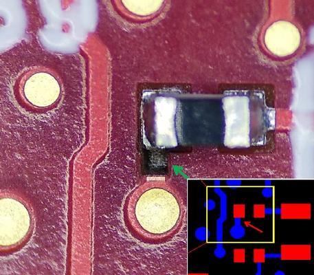
1.Vias near SMD pads: Solder can flow into the via after melted. As a result cold joint will appear in the end. Check the picture below. 2.Vias on SMD pads: Solder can flow into the via more easier after melted. Check the picture below. 3.Via opening without soldermask covered. When workers solder TH parts by hand, soldering iron can touch vias sometime, then tiny amounts molten solder will stay on vias. This can lead to electrical short easily. We recommend you make all vias tenting (covered by solder mask) if it is possible.
PCBNPI-Professional PCB Fab/PCB Assembly Service Provider From China
Technical Library | 2008-04-08 17:42:27.0
Concern about the failure of lead-free BGA packages when portable devices such as cell phones are accidentally dropped and a general concern about the resistance of these packages under shock loading has prompted an interest in the impact strength of the soldered BGA connection. This paper reports the results of the measurement of the impact strength of lead-free 0.5±0.01mm diameter BGA spheres on 0.42mm solder mask defined pads on copper/OSP and ENIG substrates using recently developed equipment that can load individual BGA spheres at high strain rates in shear and tension.
ORPRO Vision SPI Presentation. This presentation introduces the methods and technology used by ORPRO Vision in the Symbion P36 Plus SPI system. For additional information, please contact ORPRO Vision at sales.us@orprovision.com sales.eu@orprovision

SIPAD Systems Incorporated (SSi) is the Exclusive Supplier of SIPAD solid solder deposit in North America and the only SIPAD Solid Solder Deposit (SSD) coating service bureau in the world. SIPAD Systems Inc. supplies SIPAD solid solder coating servi
Events Calendar | Mon Apr 23 00:00:00 EDT 2018 - Thu Apr 26 00:00:00 EDT 2018 | Shanghai, China
SMTA China East Conference 2018
Career Center | Wellsboro, Pennsylvania USA | Engineering
SMT PROCESS ENGINEER: (Wellsboro, PA) - Designs, defines and plans the manufacturing process. Specifies and directs installation of new processes. Plans equipment build schedules and monitors vendor progress. Defines and recommends equipment, methods
| https://www.eptac.com/faqs/ask-helena-leo/ask/addressing-missing-pcb-pads-from-soldering-rework
: This is a difficult topic to answer as it has to be defined between the manufacturer and the supplier or customer. As stated, if the pads were removed during the rework process, the board was damaged and this will have to be documented and dis-positioned
Imagineering, Inc. | https://www.pcbnet.com/capabilities/fabrication/tolerances/
) The board size Tolerances on Standard Spec defined boards is +/- 0.005″ Note: We rout to your board size using the center of the board outline from the outside


