Industry Directory | Consultant / Service Provider / Manufacturer
One-stop PCBs service : Design, Manufacturing, Assembly:Low Price, Express, Quality More than 1000 electronic professionals using our services. 4 layers prototype cost up from USD 50.
Industry Directory | Consultant / Service Provider / Manufacturer
PROPOX is a manufacturer of electronics, industrial automatics, telemetric systems, tools, modules and evaluation circuits used by the constructors of electronics.
New Equipment | Assembly Services
China Double Sided Circuit Boards Fabricaiton and Assembly PCBA Turnkey Manufacturer 2 Layers circuit boards PCB FR4 1.6mm PCB fabrication and assembly 1oz PCB copper thickness Shenzhen PCB and PCBA manufacturer China turnkey contract electroni
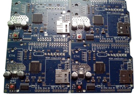
Electronics Forum | Wed Jan 07 07:50:24 EST 2009 | ludee_circuits
I think so. My customer once assembled resistors 0402 ,by Glue+wave soldering process. But PCB must be printed soldermask bridge between 0402 SMD PADs, otherwise you would encounter short problem. Sorry I don't have any comment for recommended footp
Electronics Forum | Thu Sep 10 11:47:44 EDT 2009 | mikesewell
The adhesive should be a dielectric (insulator) by design, if not it could possibly short across leads of the very parts it's intended to secure. It normally isn't a concern - what is the surface resistance of your soldermask, bodies of ICs, ...etc.
Industry News | 2019-11-05 22:07:01.0
Tenting a via refers to covering via with soldermask to enclose or skin over the opening. A via is a hole drilled into the PCB that allows multiple layers on the PCB to be connected to each other. A non tented via is just a via that is not covered with the soldermask layer. Leaving these vias exposed or covered has pros and cons depending on the your design and manufacturing requirements.
Industry News | 2019-07-09 11:16:55.0
Thanks to Ucamco’s new Gerber Job File Editor, designers can create and edit job files that provide all essential PCB production data, including essential non-image-based information, in a standard format that can be put into an automatic production flow. Ucamco’s principal aim in doing so is to make life easier for electronics design and manufacturing professionals by facilitating clear, unequivocal communications prior to production.
Technical Library | 2019-05-29 01:47:22.0
1.Vias near SMD pads: Solder can flow into the via after melted. As a result cold joint will appear in the end. Check the picture below. 2.Vias on SMD pads: Solder can flow into the via more easier after melted. Check the picture below. 3.Via opening without soldermask covered. When workers solder TH parts by hand, soldering iron can touch vias sometime, then tiny amounts molten solder will stay on vias. This can lead to electrical short easily. We recommend you make all vias tenting (covered by solder mask) if it is possible.
PCBNPI-Professional PCB Fab/PCB Assembly Service Provider From China


