Leading supplier of Solid Solder Deposit (SSD) technology and equipment to the electronics industry. Mask Tek's patented PPT process eliminates solder paste at assembly. Ideal for fine pitch and BGAs. Please visit our web site at masktek.com.
Industry Directory | Consultant / Service Provider / Manufacturer
Our Ultrasonic Stencil cleaners and 440-R-SMT Detergent are US & CA EPA Certified cleaners, that are environmentally and user safe. We are your single source for cleaning any type of solder paste from any fine pitch stencil.
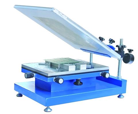
TP300 is the simplest solution, the most compact-size and lowest-cost solder paste printer, it can be easy and accurate to print the solder paste on any board. Please see details below: 1). It is suitable for both single-sided and double-sided p
New Equipment | Solder Paste Stencils
We use fine grain stainless steel for the base of all our Stencils, All Stencils are cut on LPKF lasers which ensures the best quality for optimum paste release. Our Stencils are offered in thicknesses from .0015" to .0020". Our laser cut Stencils c
Electronics Forum | Sat Aug 21 02:27:21 EDT 2010 | isd_jwendell
The paste you dispense will not solder the same as the one you use with a stencil. The paste for the stencil will have a higher metal content. I was not working with dispensing as small as you are, but after evaluating the cost of the stencil vs. lon
Electronics Forum | Mon Aug 16 14:43:44 EDT 2010 | dan_ems
Hello, i don't know if is possible to dispense paste but for reduction of cost we use a diferent type of stencils, from aluminium of 0,2 mm, purchased from a typography of newspapers. Ofcourse the pcb for what we use this stencil are simple. But th

Used SMT Equipment | SMT Equipment
Product Name :Panasoinc NPM module Product number: two modules NPM Detailed product introduction 2D inspection head function of NPM tape coating machine: 1, NPM check head resolution: 9 m 2, NPM check head vision: 21.1 * 17.6mm 3, check proc
Used SMT Equipment | SMT Equipment
Product Name :Panasoinc NPM module Product number: two modules NPM Detailed product introduction 2D inspection head function of NPM tape coating machine: 1, NPM check head resolution: 9 m 2, NPM check head vision: 21.1 * 17.6mm 3, check proc
Industry News | 2003-03-21 08:12:24.0
Tecan reckons it is consistently producing what may be regarded as the most efficient stencils in the world today.
Industry News | 2008-03-25 23:53:54.0
Comment from Brian D�Amico, President
Parts & Supplies | Pick and Place/Feeders
Expert-SAFP (110V/230V configurable) NEW PRICE EUR30.000,-, now for EUR 18.500 net (excl. Tax) only. Perfect for fast and reliable Prototyping. For sale is an Essemtec Expert-SAFP (110V/230V configurable). The Expert-SAFP is a professinal semi-
Technical Library | 2019-05-23 10:30:22.0
Increasing I/O numbers, device complexity, and product miniaturization requires high precision bonding tools, and sophisticated equipment. Careful consideration should be given to wedge geometry while selecting the tool for a fine pitch wire bonding application. Wire bonding is a process that creates an electrical connection between a die and a substrate or lead typically using gold or aluminum wire. Wedge bonding is a specific type of wire bonding that uses a wedge shaped tool to create the welds. The design of the wedge tool has changed very little over the past decade. The wire is fed at an angle through the back of the wedge. This angle is typically 30 to 60 degrees and is application dependent. Some applications require a higher feed angle due to package clearance issues. Some deep access applications require a 90 degree feed angle. In this configuration, the wire is fed through a hole in the shank of the wedge tool. Wire feed is shown in Figure 1.
Technical Library | 2023-07-25 16:50:02.0
Some of the new handheld communication devices offer real challenges to the paste printing process. Normally, there are very small devices like 01005 chip components as well as 0.3 mm pitch uBGA along with other devices that require higher deposits of solder paste. Surface mount connectors or RF shields with coplanarity issues fall into this category. Aperture sizes for the small devices require a stencil thickness in the 50 to 75 um (2-3 mils) range for effective paste transfer whereas the RF shield and SMT connector would like at least 150 um (6 mils) paste height. Spacing is too small to use normal step stencils. This paper will explore a different type of step stencil for this application; a "Two-Print Stencil Process" step stencil. Here is a brief description of a "Two-Print Stencil Process". A 50 to 75 um (2-3 mils) stencil is used to print solder paste for the 01005, 0.3 mm pitch uBGA and other fine pitch components. While this paste is still wet a second in-line stencil printer is used to print all other components using a second thicker stencil. This second stencil has relief pockets on the contact side of the stencil any paste was printed with the first stencil. Design guidelines for minimum keep-out distances between the relief step, the fine pitch apertures, and the RF Shields apertures as well relief pocket height clearance of the paste printed by the first print stencil will be provided.

SMT is surface assembly technology, a new generation of electronic assembly technology developed from hybrid integrated circuit technology. SMT production line is also called surface assembly technology. Full-auto SMT Production Line is a new generat
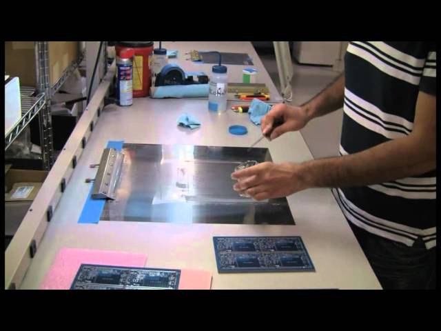
This is video shows how to print a PCB using a prototype foil only stencil. The SMT prototype stencil (www.soldertools.net) is made from a high nickel content material able to offer repeatable high precision apertures. The steps of alignment, printin
Training Courses | | | PCB Rework and Hand Soldering Courses
The PCB rework and hand soldering courses courses cover techniques of rework and repair of PCBs, BGAs and other electronics assemblies, and teach fundamentals of soldering of electronics assemblies.
Training Courses | | | PCB Rework and Hand Soldering Courses
The PCB rework and hand soldering courses courses cover techniques of rework and repair of PCBs, BGAs and other electronics assemblies, and teach fundamentals of soldering of electronics assemblies.
Events Calendar | Mon Mar 18 00:00:00 EDT 2019 - Mon Mar 18 00:00:00 EDT 2019 | ,
Webinar: Stencil Design for Solder Paste, In Process Inspection & Process Defects
Events Calendar | Wed May 31 00:00:00 EDT 2023 - Wed May 31 00:00:00 EDT 2023 | Holtsville, New York USA
Long Island Chapter Meeting: Fine Feature Paste Printing, Stencil Design and Solder Technology
Career Center | Gwinnett County, Georgia USA | Production
SHIFTS: 1st and 2nd Shifts (Over-Time as required) STATUS: Indefinite Temporary PAY: $11.00-$12.00 per hour JOB DESCRIPTION • Perform SMT soldering, desoldering, rework, and assembly of fine pitch electronic components on Printed Circuit Boards (PCB
Career Center | , Israel | Engineering,Maintenance,Technical Support
I was born on June , 1972 in Khmelnitsky city , Ukraine . I am male. From 1979 to 1987 I was studying at secondary school #7, having finished which I entered the Technical College of Khmelnitsky in specialty Machine Tools with Computer Numeric Contr
Career Center | ORLANDO, Florida USA | Engineering,Maintenance,Production,Technical Support
Manufacturing tech/eng for a contract manufacture for 10+ years. Been working in the SMT industry for a total of 20yrs. Have done everything from operator to process work. Most familiar with Assembleon, MPM, DEK, BTU,Electrovert, SLIM-KIC, SUPER-MOLE
Sustaining a Robust Fine Feature Printing Process Sustaining a Robust Fine Feature Printing Process With the introduction of 01005 chip components and 0.3 mm pitch CSP devices, electronic component packaging is pushing surface mount technology
ASYMTEK Products | Nordson Electronics Solutions | https://www.nordson.com/en/divisions/efd/blog/031919-super-glue-dispensing-101
, EFD’s Ultimus II dispenser offers the best control for thin super glues. You can fine-tune time and pressure adjustments to dispense the right amount
PCB Libraries, Inc. | https://www.pcblibraries.com/forum/advice-for-solder-mask-paste-mask-layers_topic484_page1.html
. These are for example: 1. Solder mask defined pads under fine pitch BGA packages. 2. Multiple separated squares on the paste mask layer to create 50


