Industry Directory | Consultant / Service Provider
PCB assembly services, both US and offshore. We handle basic through-hole to standard surface mount to ultra-fine pitch. Quote and order PCB fabrication and assembly online.

The PCB Footprint Expert is a powerful CAD library development tool powered by our own proprietary CAD LEAP Technology (Libraries Enhanced with Automated Preferences). It is packed with very powerful advanced library management features that cuts foo

Layer: 2 Material: FR-4 Board Thickness: 1.6mm Surface Finish: HAL Copper Thickness: 2/2 oz Green Solder Mask Layers: 2--36layers Max manufacturing size: 640mm*1100mm Copper foil thickness: 0.5OZ-13OZ Min line width/space: 3mil/3mil Min
Electronics Forum | Tue Sep 25 14:08:59 EDT 2001 | davef
Oooo, the solder on the pad and PGA ball is flowing during reflow down the via to the secondary side? Why didn�t you say so?? ;-) Why would you expect that gravity and capillary action wouldn�t force solder to flow down the solder plated via to the
Electronics Forum | Fri Mar 26 17:12:17 EST 2004 | ben
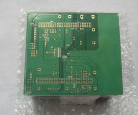
I have recently encountered a new pcb design with a very high density of components on either side of the pcb. One of the suggested "fixes" is to use the smt pads as vias i.e. the via will be drilled thorough the centre of the smt pad. My concern i
Industry News | 2018-08-16 19:58:50.0
The SMTA Capital Chapter is holding its upcoming Capital Expo and Tech Forum at Johns Hopkins University / Applied Physics Lab, Kossiakoff Center, 11100 Johns Hopkins Road, Laurel, MD 20723, on Thursday, August 23rd.
Parts & Supplies | Circuit Board Assembly Products
1). 100mm x 98mm/1up, FR-4, 2). 1mm +/-0.1mm,6 Layers 3). 1oz copper finished 3). Green solder mask/white legend 4). Min. hole 0.15mm, 4/4 mil track/gap 5). Blind via layer 1-2, via-in-pad. 6). Immersion gold surface finish
Technical Library | 2019-10-10 00:26:28.0
Voids are a plague to our electronics and must be eliminated! Over the last few years we have studied voiding in solder joints and published three technical papers on methods to "Fill the Void." This paper is part four of this series. The focus of this work is to mitigate voids for via in pad circuit board designs. Via holes in Quad Flat No-Lead (QFN) thermal pads create voiding issues. Gasses can come out of via holes and rise into the solder joint creating voids. Solder can also flow down into the via holes creating gaps in the solder joint. One method of preventing this is via plugging. Via holes can be plugged, capped, or left open. These via plugging options were compared and contrasted to each other with respect to voiding. Another method of minimizing voiding is through solder paste stencil design. Solder paste can be printed around the via holes with gas escape routes. This prevents gasses from via holes from being trapped in the solder joint. Several stencil designs were tested and voiding performance compared and contrasted. In many cases voiding will be reduced only if a combination of mitigation strategies are used. Recommendations for combinations of via hole plugging and stencil design are given. The aim of this paper is to help the reader to "Fill the Void."
Technical Library | 2023-01-10 20:15:42.0
Over the past years there has been consistent growth in the use of electroless nickel / immersion gold (ENIG) as a final finish. The finish is now frequently being used for PBGA, CSP, QFP and COB and more recently gathered considerable interest as a low cost under-bump metallization for flip chip bumping application. One of the largest users for this finish has been the telecommunication industry, were millions of square meters of PCBs with ENIG have been successfully used. The nickel layer offers advantages such as multiple soldering cycles and hand reworks without copper dissolution being a factor. The nickel also acts as a reinforcement to improve through-hole and blind micro via thermal integrity. In addition the nickel layer offers advantages such as co-planarity, Al-wire bondability and the use as contact surface for keypads or contact switching. Especially those pads, which are not covered by solder need a protective coating in corrosive environment – such as high humidity or pollutant gas.

The PCB Footprint Expert is a powerful CAD library development tool powered by our own proprietary CAD LEAP Technology (Libraries Enhanced with Automated Preferences). It is packed with very powerful advanced library management features that cuts foo

Teaching video on PCB through hole repair. BEST instructors teach the method for repair of a damaged eyelet using a multitude of different close up and angled views. Repair is completed per the IPC 7721 instructions. http://www.solder.net
Training Courses | | | PCB Assembly Courses
The PCB assembly courses provide knowledge of different processes and equipment used in TH and SMT assembly of printed circuit boards.
SMT Express, Volume 2, Issue No. 3 - from SMTnet.com Volume 2, Issue No. 3 Thursday, March 16, 2000 Featured Article Return to Front Page Stencil Design for Mixed Technology Through-hole / SMT Placement and Reflow by William E. Coleman, Photo
Heller Industries Inc. | https://hellerindustries.com/opensor-insufficient-solder/
stencil aperture Misaligned solder print Improper stencil thickness Inadequate stencil aperture size Excessive pad size Via in pad draining solder from interconnection Reflow-related causes of
| https://pcbasupplies.com/solder-tip-cleaners/
& Place Nozzles Clearance Solder Products Brands Thermaltronics XDry Corp Count On Tools Quantum Storage Systems PCBASupplies BEAU TECH EasyBraid Tronex Koki Categories Hand Soldering

COT specializes in high quality SMT nozzles and consumables for pick and place machines. We provide special engineering design service of custom nozzles for those unique and odd components.
2481 Hilton Drive
Gainesville, GA USA
Phone: (770) 538-0411

.gif)


