
Industry Directory | Training Provider / Manufacturer's Representative / Equipment Dealer / Broker / Auctions / Consultant / Service Provider
Products, services, training & consulting for the assembly, rework & repair of electronic assemblies. BGA process experts. Manufacturers Rep, Distributor & Service Provider for Seamark/Zhuomao and Shuttle Star BGA Rework Stations.
Industry Directory | Manufacturer
Reflow ovens for automated SMT PCB assembly, specializing in lead free processing and nitrogen reflow. The best convection reflow ovens on the market.
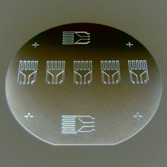
New Equipment | Solder Paste Stencils
MLT stainless steel and non-metal stencils (i.e. Kapton) are laser fabricated for applying solder paste, flux, solderballs, to circuit boards, wafers, and components for prototypes, volume production, and PCB rework.
Electronics Forum | Fri Oct 24 06:55:48 EDT 2008 | clampron
Good Morning WS, If you experieced the solder balls after reflow of a bare board through the oven, then the source of the solder is either the oven or the board. I have had boards with untented via's that were HASL'd that had entrapped solder and fl
Electronics Forum | Mon Oct 27 14:15:47 EDT 2008 | hussman
So you passed a BARE board thru the oven and got solder balls?
Industry News | 2003-04-30 08:51:08.0
Electrolube played the role of environmental champion in Australia recently.
Industry News | 2023-04-11 09:52:04.0
MIRTEC will premier its complete line of 3D AOI and SPI Inspection Systems at SMTconnect, scheduled to take place May 9-11, 2023 in Nuremberg, Germany. The company will showcase a total of five (5) Inspection Systems specifically designed to address the full spectrum of inspection requirements associated with the electronics manufacturing industry in Hall 4A, Stand 128.

Parts & Supplies | Pick and Place/Feeders
Many companies first applied SMT second-hand placement machines, and the selected placement machines were relatively stable, with low failure rate, easy maintenance, and important maintenance costs. Therefore, there are still many concerns about buyi
Parts & Supplies | Pick and Place/Feeders
Many companies first applied SMT second-hand placement machines, and the selected placement machines were relatively stable, with low failure rate, easy maintenance, and important maintenance costs. Therefore, there are still many concerns about buyi
Technical Library | 2013-04-11 15:43:17.0
With the explosion of growth in handheld electronics devices, manufacturers have been forced to look for ways to reinforce their assemblies against the inevitable bumps and drops that their products experience in the field. One method of reinforcement has been the utilization of underfills to "glue" certain SMDs to the PCB. Bumped SMDs attached to the PCB with a no-clean soldering process offer the unavoidable scenario of the underfill coming in contact with a flux residue. This may or may not create a reliability issue... First published in the 2012 IPC APEX EXPO technical conference proceedings
Technical Library | 2015-12-31 15:19:28.0
Today's consumer electronic product are characterized by miniatuization, portability and light weight with high performance, especially for 3G mobile products. In the future more fine pitch CSPs (0.4mm) component will be required. However, the product reliability has been a big challenge with the fine pitch CSP. Firstly, the fine pitch CSPs are with smaller solder balls of 0.25mm diameter or even smaller. The small solder ball and pad size do weaken the solder connection and the adhesion of the pad and substrate, thus the pad will peel off easily from the PCB substrate. In addition, miniature solder joint reduce the strength during mechanical vibration, thermal shock, fatigue failure, etc. Secondly, applying sufficient solder paste evenly on the small pad of the CSP is difficult because stencil opening is only 0.25mm or less. This issue can be solved using the high end type of stencil such as Electroforming which will increase the cost.
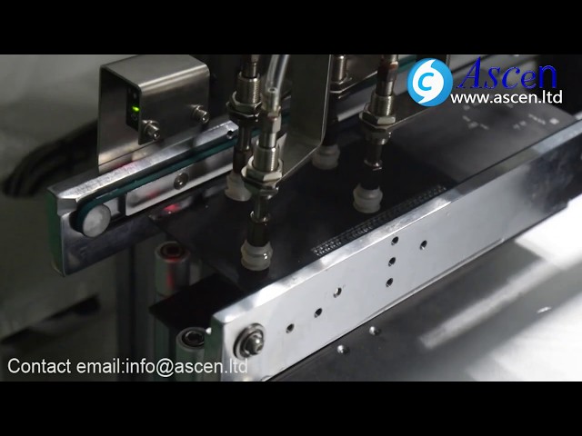
PCB vacuum suction loader/SMT vacuum loader for loading bare board on PCB assembly line: https://www.ascen.ltd/Products/Automatic_SMT_equipment/PCB_loader/123.html ASCEN PCB vacuum loader we produced is mainly used for the beginning of the SMT produc
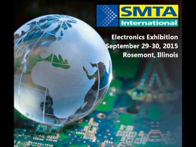
SMTA International Electronics Exhibition Tuesday, September 29: 9am-5pm Wednesday, September 30: 9am-4pm Donald Stephens Convention Center Rosemont, IL See More Equipment & Technology Than Ever Before! Many of the 160 exhibiting companies will bri
Training Courses | | | PCB Design Courses
The PCB design courses teach students the process, techniques and tools needed to design layout of printed circuit boards.
Events Calendar | Sun Sep 27 00:00:00 EDT 2020 - Thu Oct 01 00:00:00 EDT 2020 | Rosemont, Illinois USA
SMTA International 2020 Conference & Exhibition
Events Calendar | Mon Apr 23 00:00:00 EDT 2018 - Thu Apr 26 00:00:00 EDT 2018 | Shanghai, China
SMTA China East Conference 2018
Career Center | Sherman, Texas USA | Engineering,Production,Research and Development,Technical Support
SMT Packaging Engineer: Location: Texas - Sherman , TX Group: HVAL Degree Requirements: BS ME/ChemE/Materials The person in this position will have the ability to make very significant financial contributions to TI because this is a very critic
Career Center | NORTHRIDGE, California USA | Engineering
EDUCATION BS Electronics and Communication Engineering Gujarat University MS Electrical Engineering California State University, Northridge ACADAMIC PROJECT Fabrication and Characterization of Silicon Carbide (SiC) MESFE
Career Center | Botevgrad, Sofia Bulgaria | Engineering,Production,Quality Control,Research and Development,Sales/Marketing
AOI - Omron RNS/RNS_ptH, VI3000, Marantz 22X IPC-610D Class 3, Pb/Pb free process, 5S, FMEA, MSA, PPAP, SPC, CPK, 6Sigma, lean manufacturing, Quality management, ISO/TS 16949 ,ISO 9001,ISO 14 001
Reliability Enhancement of Wafer Level Packages with Nano-Column-Like Hollow Solder Ball Structures Reliability Enhancement of Wafer Level Packages with Nano-Column-Like Hollow Solder Ball Structures by: Ronak Varia, Xuejun Fan; Lamar University
Heller Industries Inc. | https://hellerindustries.com/intermetallics-growth/
& Technical Articles Videos THERMAL PROCESS SOLUTIONS Reflow Soldering Solutions Causes & Defects – Reflow Soldering Solder Ball Defects Insufficient Solder Wicking Defects Tombstoning PCB Soldering PCB Bridging Defects PCB Dewetting PCB Nonwetting Circuit Board Voids Intermetallic Growth on PCB
| http://etasmt.com/cc?ID=te_news_bulletin,23575&url=comment
Intermetallic Growth on PCB-News-Reflow oven,SMT Reflow Soldering Oven-cmsadmin Home About I.C.T News Products Video Projects Service Join Us Contact Us Home About I.C.T
Products, services, training & consulting for the assembly, rework & repair of electronic assemblies. BGA process experts. Manufacturers Rep, Distributor & Service Provider for Seamark/Zhuomao and Shuttle Star BGA Rework Stations.
Training Provider / Manufacturer's Representative / Equipment Dealer / Broker / Auctions / Consultant / Service Provider
1750 Mitchell Ave.
Oroville, CA USA
Phone: (888) 406-2830


