Industry Directory | Manufacturer
Reflow ovens for automated SMT PCB assembly, specializing in lead free processing and nitrogen reflow. The best convection reflow ovens on the market.
Industry Directory | Manufacturer
Industrial Sensor Vision International specializes in advanced camera technology of high resolution fast speed cameras for automation, AOI, 2-D/3-D, SPI inspection and wafer inspection.
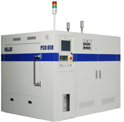
New Equipment | Curing Equipment
A Pressure Cure Oven (PCO), or Autoclave, is used to minimize voiding and increase adhesion strength for bonding processes typically used in die attach and underfill applications. PCO pressurizes air into a rigid vessel and heats & cools with

Flux Free Formic Reflow Reflow in Formic Acid Vapor Heller has designed and built an production ready horizontal reflow oven for formic acid vapor. This new oven has been designed to meet Semi S2/S8 safety standards (including toxic gases). Form
Electronics Forum | Fri Nov 10 12:22:12 EST 2000 | casi
I'm interested in probes for wafer testing made in verted. I need to tested wafers with pad with flat gold bumps ( 17um ) with pitch = 70um. I'm also interested in every web site related on gold bumps testing. Thanks a lot !!! Casi
Electronics Forum | Mon Jun 05 05:41:48 EDT 2000 | casi
I need to find info about testing and probe contact about wifers with bump on pads. Thanks a lot to everybody that helps me
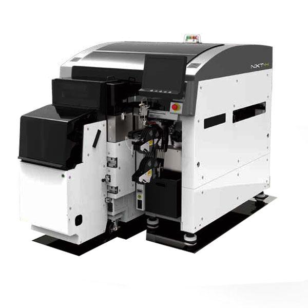
Used SMT Equipment | Chipshooters / Chip Mounters
NXT-H and NXT-Hw support placing small LEDs and bare dies at high-speed as well as performing hybrid production including flip chips.Fuji Ultra Accurate Placement Platform.Hybrid placement of wafers and SMDs. Wafer and reel part placement in a single
Industry News | 2021-06-26 09:04:13.0
Whizz Systems, Inc. today announced the addition of a Powersonic™ Benchtop Ultrasonic Cleaner from Crest Ultrasonics.
Industry News | 2003-01-27 10:27:31.0
At a New Facility Within the Company's U.S. Headquarters
Parts & Supplies | Pick and Place/Feeders
Wafer-Feeder Kabel X11 25pol. Sub.D
Technical Library | 2020-01-28 00:23:58.0
This paper explores new advances in the reflow soldering process including vacuum technology and warpage mitigation systems. The first topic for discussion will be the implementation of a vacuum process directly in a conventional inline soldering system. The second topic presented is the mitigation of warpage on substrates or wafers.
Technical Library | 2010-06-23 21:59:03.0
Quality control is one of the main bottlenecks in the production of micro-opto-electromechanical systems/microelectromechanical systems (MOEMS/MEMS) because each structure on a wafer is serially inspected and scanned stepwise over the entire wafer area.
General curing, die attach curing, underfill curing, film & tape bonding, wafer laminating.
Nano-copper sintering in formic acid vapor.
Training Courses | | | PCB Design Courses
The PCB design courses teach students the process, techniques and tools needed to design layout of printed circuit boards.
Events Calendar | Tue Feb 15 00:00:00 EST 2022 - Thu Feb 17 00:00:00 EST 2022 | San Jose, California USA
Wafer-Level Packaging Symposium
Events Calendar | Fri Sep 18 00:00:00 EDT 2020 - Fri Sep 18 00:00:00 EDT 2020 | ,
Defect Detection for Advanced Wafer and Package Devices
Career Center | Santa Cruz, California USA | Research and Development,Sales/Marketing
Project and Application Development Manager. Seeking seasoned project manager, with communications ability, sales savvy and experience with wafer singulation, lasers, or semiconductor packaging. Role will encompass all aspects of project management
Career Center | Santa Cruz, California USA | Research and Development,Sales/Marketing
Seeking seasoned Applications Engineer, with communications ability, sales savvy and experience with wafer singulation, lasers, or semiconductor packaging. Role will encompass all aspects of Applications development and Customer Field service involvi
Career Center | NORTHRIDGE, California USA | Engineering
EDUCATION BS Electronics and Communication Engineering Gujarat University MS Electrical Engineering California State University, Northridge ACADAMIC PROJECT Fabrication and Characterization of Silicon Carbide (SiC) MESFE
Career Center | Melbourne, Florida USA | Management,Production,Quality Control
Technical Skills/Abilities: � Management � Quality Assurance � Strong Troubleshooting Skills � Strategic Planning � Employee Training � Quality Assurance � Problem Resolution � Mechanical/Technical Aptitude
Reliability Enhancement of Wafer Level Packages with Nano-Column-Like Hollow Solder Ball Structures Reliability Enhancement of Wafer Level Packages with Nano-Column-Like Hollow Solder Ball Structures by: Ronak Varia, Xuejun Fan; Lamar University


