
BGA Heat Sink (High Aspect Ratio Ext.) High efficiency pin fin design provides low pressure drop characteristics Large surface area increases heat sink performance Fabricated from extruded aluminum, which minimizes thermal resistance fro

New Equipment | Assembly Services
Quick turn Prototype PCBs from 24 hour turnaround to high volume printed circuit board production from our domestic plant in USA and/or China facilities. Our Modern 38,000 sq. ft. manufacturing plant with multi-million dollar investment with latest e
Electronics Forum | Wed Mar 28 11:29:49 EST 2001 | gcs
I've used below: WEIGTH OF COMPONENT IN GRAMS ---------------------------- TOTAL PAD MATING AREA IN SQUARE INCHES GRAMS PER SQUARE INCH MUST BE EQUAL/GREATER THAN 30 FOR SECONDARY MOUNTING.
Electronics Forum | Thu Oct 15 11:04:28 EDT 2009 | spitkis2
Thanks Jim. Pressing the QFN into paste was what I thought of, just wasn't sure if it would cause solder paste to be pressed outside the pad area and possibly bridge with an adjacent pad. Do you recall the ratio of paste coverage to the pad area?
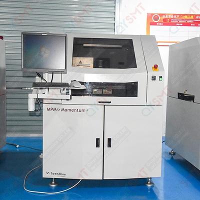
Used SMT Equipment | Screen Printers
Momentum was designed and built to be a no-nonsense production machine. Cost-efficient and featuring a modest footprint, it grows with the user; innovative patented features can be added on or retrofitted as needed as the user’s throughput dema
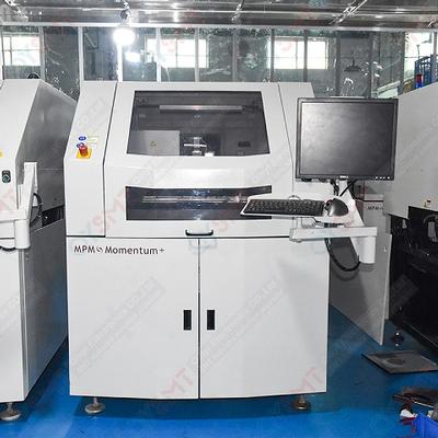
Used SMT Equipment | Screen Printers
Momentum was designed and built to be a no-nonsense production machine. Cost-efficient and featuring a modest footprint, it grows with the user; innovative patented features can be added on or retrofitted as needed as the user’s throughput dema
Industry News | 2018-12-08 03:29:29.0
SMT Dictionary – Surface Mount Technology Acronym and Abbreviation

Parts & Supplies | SPI / Solder Paste Inspection
Quick programming, friendly programming interface Multiple measurement methods True one-button measurement Eight-way motion button, one-click focus Adjustable scanning pitch Solder paste 3D simulation function Powerful SPC function MARK
_1.jpg)
Parts & Supplies | Pick and Place/Feeders
JUKI FEEDER part E513070600B E9630729000 T AC SERVO MOTOR(TS4632N2020E600) E9630755000 RERAY UNIT E96307800A0 HEAD SENSOR ASM E963171500A DUCT (KD-76-03-C) E963171500B DUCT (KD-76-045-C) E963171500C DUCT (KD-76-085-C) E9631721000 LAHD SENSOR
Technical Library | 2017-09-28 16:36:33.0
These nano-coatings also refine the solder paste brick shape giving improved print definition. These two benefits combine to help the solder paste printing process produce an adequate amount of solder paste in the correct position on the circuit board pads. Today, stencil aperture area ratios from 0.66 down to 0.40 are commonly used and make paste printing a challenge. This paper presents data on small area ratio printing for component designs including 01005 Imperial (0402 metric) and smaller 03015 metric and 0201 metric chip components and 0.3 mm and 0.4 mm pitch micro BGAs.

Inline 3D SPI, Standard Automatic solder paste inspection system As one of the strongest SMT 3D SPI Manufacuturer in China, we provide you all the different models of online solder paste inspection machine,we have variety of size and models of the
Substrate processing: Maximum substrate size (XxY): 609.6mmx508mm(24”x20”) For circuit boards larger than 20”, special fixtures are required Minimum substrate size (XxY): 50.8mmx50.8mm(2”x2”)
Career Center | Bangalore, India | Engineering,Maintenance,Production,Technical Support
SMT Stencil designing & Knowledge of full SMT process software known CAD/CAM -circuit CAM Pro 7.3,GC Power station, GCCAM Edit,Auto CAD, Fault finding of Electronic Boards & Servicing electronic machines.
SMTnet Express, September 28, 2017, Subscribers: 30,862, Companies: 10,741, Users: 23,873 An Investigation into the Use of Nano-Coated Stencils to Improve Solder Paste Printing with Small Stencil Aperture Area Ratios Jasbir Bath, Tony Lentz, Greg


