Industry Directory | Manufacturer
Nepes offers flip chip solutions ranging from wafer bumping to advanced packaging and testing for IC manufactures, module electronics and end-product makers.
Industry Directory | Consultant / Service Provider
CAD Design Software products run in the AutoCAD environment.
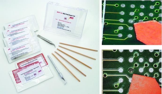
New Equipment | Rework & Repair Equipment
The BEST PCB pad repair repair kit gives you the tools you need for fast modification and repair of PCB circuit pads-no matter what their size. Our online PCB repair training videos, our master instructors along with these materials allows you to mee
New Equipment | Rework & Repair Equipment
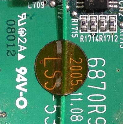
BEST HotDots™ are designed to simply and cleanly attach jumper wires on a board. HotDots™ are built to survive at high temperature as both the adhesive and the polyimide material are designed to withstand wash and reflow temperatures. HotDots™ are a
Electronics Forum | Fri Jan 20 02:34:16 EST 2006 | yihui
Hi, i'm david, new to this forum. Came across your posting about using a delvotec bonder to TS bond to a ENIG pad. Given that the immersion gold layer is thin, does the capillary scrub through the gold layer to expose the underlying nickel? Does your
Electronics Forum | Sun May 26 10:21:46 EDT 2002 | V.RAMANAND KINI
We buy PCBs for aluminium wire bonding. Our PCBs have 0.25 mm square pads for bonding and 0.10 or 0.15 mm gap between circuit traces/tracks. We do not have any problem. Our vendor gives 9 microns of Nickel and 0.03 microns of gold.

Used SMT Equipment | X-Ray Inspection
Very Nice Nicolet Xray Machine For Sale The system is complete and in good working condition See attached pictures and information below Nicolet Imaging Systems Model Number: NXR-1500 Serial Number: 0150011 Year 2000 Variable Speed Joystick
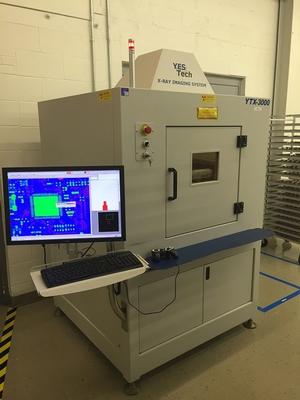
Used SMT Equipment | X-Ray Inspection
Yestech High Resolution Imaging PCB Xray Serial Number: X10706656 Model Number: YTX 3000 Year 2007-2008 130 KV XrayTube with 5 micron spot size Xray on Hours - 18.2 Standby Hours - 328.5 Measured Filament - 2.22 Hamamatsu L19181-02 Sam
Industry News | 2015-11-25 16:58:05.0
On behalf of the SMTA International Technical Committee, we invite you to submit a 300 word abstract of your research for the 2016 SMTA International 2016 technical conference in Rosemont, Illinois. Papers should describe significant results from experiments, emphasize new techniques, and contain technical, economic or appropriate test data. We are looking for papers on a variety of topics related to electronics manufacturing including advanced packaging/components, assembly, business/supply chain, emerging technologies, harsh environment applications, PCB technology, and process control. Materials must be original, unpublished and non-commercial in nature.
Parts & Supplies | Circuit Board Assembly Products
PULANG TECHNOLOGY CO,.LTDOffers electronic manufacturing services including PCB designing, electronic contract manufacturing including electronic product design, electronic product development, electronic product repair, PCB manufacturing, electronic
Parts & Supplies | Chipshooters / Chip Mounters
Below universal auto insertion parts are Manufactured in China,so no need to describe too much about price,what's the difference is that you will surely like it when you try them on machines,just based on the proved quality,please contact louis@smt-m
Technical Library | 2007-01-31 15:17:04.0
The goal of this project is to evaluate the reliability of lead-free BGA solder joints with a variety of different pad sizes using several different BGA rework methods. These methods included BGAs reworked with both flux only and solder paste attachment techniques and with or without the use of the BEST stay in place StencilQuick™. The daisy chained test boards were placed into a thermal test chamber and cycled between -25ºC to 125ºC over a 30 minute cycle with a 30 minute dwell on each end of the cycle. Each BGA on the board was wired and the continuity assessed during the 1000 cycles the test samples were in the chamber.
Technical Library | 2020-08-27 01:22:45.0
Initially adopted internal specifications for acceptance of printed circuit boards (PCBs) used for wire bonding was that there were no nodules or scratches allowed on the wirebond pads when inspected under 20X magnification. The nodules and scratches were not defined by measurable dimensions and were considered to be unacceptable if there was any sign of a visual blemish on wire-bondable features. Analysis of the yield at a PCB manufacturer monitored monthly for over two years indicated that the target yield could not be achieved, and the main reasons for yield loss were due to nodules and scratches on the wirebonding pads. The PCB manufacturer attempted to eliminate nodules and scratches. First, a light-scrubbing step was added after electroless copper plating to remove any co-deposited fine particles that acted as a seed for nodules at the time of copper plating. Then, the electrolytic copper plating tank was emptied, fully cleaned, and filtered to eliminate the possibility of co-deposited particles in the electroplating process. Both actions greatly reduced the density of the nodules but did not fully eliminate them. Even though there was only one nodule on any wire-bonding pad, the board was still considered a reject. To reduce scratches on wirebonding pads, the PCB manufacturer utilized foam trays after routing the boards so that they did not make direct contact with other boards. This action significantly reduced the scratches on wire-bonding pads, even though some isolated scratches still appeared from time to time, which caused the boards to be rejected. Even with these significant improvements, the target yield remained unachievable. Another approach was then taken to consider if wire bonding could be successfully performed over nodules and scratches and if there was a dimensional threshold where wire bonding could be successful. A gold ball bonding process called either stand-off-stitch bonding (SSB) or ball-stitch-on-ball bonding (BSOB) was used to determine the effects of nodules and scratches on wire bonds. The dimension of nodules, including height, and the size of scratches, including width, were measured before wire bonding. Wire bonding was then performed directly on various sizes of nodules and scratches on the bonding pad, and the evaluation of wire bonds was conducted using wire pull tests before and after reliability testing. Based on the results of the wire-bonding evaluation, the internal specification for nodules and scratches for wirebondable PCBs was modified to allow nodules and scratches with a certain height and a width limitation compared to initially adopted internal specifications of no nodules and no scratches. Such an approach resulted in improved yield at the PCB manufacturer.

ACI Technologies Inc. (ACI) is a scientific research corporation dedicated to the advancement of electronics manufacturing processes and materials for The Department of Defense and industry. This video provides an overview of our commercial service
Ultra-flexible, offline, multi-platform, quick load twin PCB rotary table selective soldering system Designed to meet the needs of the small batch manufacturer who requires high levels of production flexibility. The Jade Prodex offers the ability to
Training Courses | | | IPC-7711/7721 Specialist (CIS)
The Certified IPC-7711/7721 Specialist (CIS) training focuses on rework of electronic assemblies and repair and modification of printed boards and electronic assemblies.
Training Courses | | | IPC-7711/7721 Trainer (CIT)
The Certified IPC-7711/7721 Trainer (CIT) courses recognize individuals as qualified trainers in the area of rework and repair of printed boards and electronic assemblies and prepares them to deliver Certified IPC-7711/7721 (CIS) training.
Events Calendar | Mon Apr 23 00:00:00 EDT 2018 - Thu Apr 26 00:00:00 EDT 2018 | Shanghai, China
SMTA China East Conference 2018
Career Center | Brooklyn, New York USA | Engineering,Production
Mini-Circuits designs, manufactures and distributes integrated circuits, modules, and sub-systems for high performance radio frequency (RF) and microwave applications. With design, sales and manufacturing locations in over 30 countries, Mini-Ci
SMT Express, Volume 2, Issue No. 9 - from SMTnet.com Volume 2, Issue No. 9 Thursday, September 14, 2000 Featured Article Return to Front Page Book Review Reviewed by Dave Fish (davef ), Pandion Electronics, Inc Title: Wire Bonding
ASYMTEK Products | Nordson Electronics Solutions | https://www.nordson.com/en/industries/electrical?con=t&page=6
) instructions Assembly Using X-Wire™ Insulated Bonding Wire Technology Nordson MARCH Wearing a wire? Wearable electronics present exciting opportunities for human-technology interaction Nordson DAGE 5th March, 2021 Stellar 4000 datasheet Nordson DAGE First
GPD Global | https://www.gpd-global.com/pdf/lead-former/CF8-Wire-Clamp-Replacement-8201622.pdf
. Install horizontal or modified horizontal dies of any size in stations 6 & 7. 2. Place slid assembly (PN 801-1-200) in die block. 3. Inspect wire clamp-to-die alignment


