
The PCB Footprint Expert is a powerful CAD library development tool powered by our own proprietary CAD LEAP Technology (Libraries Enhanced with Automated Preferences). It is packed with very powerful advanced library management features that cuts foo
New Equipment | Rework & Repair Services
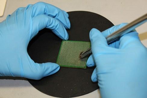
BGA Reballing Services BEST provides BGA reballing services for your plastic-, ceramic- and metalbodied components down to 0.3mm pitch. We have the ability to develop the BGA reballing process you want with a variety of deballing methods and machine
New Equipment | Solder Paste Stencils
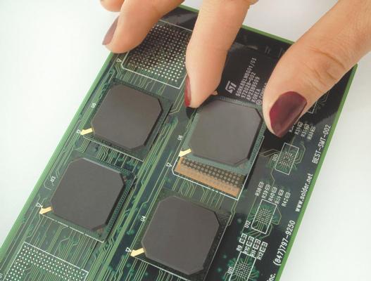
Eliminate hours of solder mask damage repair time for bga sites while improving rework yield. Are you frustrated by the time it takes to repair mask damage underneath the BGA during the rework process? Are you squeezed for space on the PCB in an
New Equipment | Solder Materials
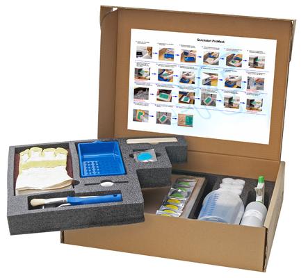
An easy-to-use cost-effective solution for producing professionally masked PCBs in an in-house prototyping environment. Compact, quick and easy to use Professional finish and perfect soldering Four simple steps to a professional result

The high-end system in the series is the INSIGNUM 4000 Laser which exhibits the highest precision at an impressive cycle time of less than 4.8 seconds. The ASYS inline Laser marking system, INSIGNUM 4000 Laser, is used for direct laser marking of so
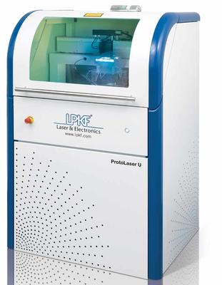
The next generation of in-house prototyping Laser-based PCB production can achieve much greater circuit detail, and lasers structure circuits significantly faster. This technology provides true on-demand production solution for both prototyping and
New Equipment | Solder Paste Stencils
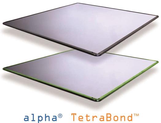
ALPHA® Stencil products are based on unique blends of advanced technology, the experience gained from having made over half a million solder paste stencils, the specialist knowledge that could only be accumulated by a company privileged to produce bo
New Equipment | Board Handling - Pallets,Carriers,Fixtures
* Provides dimensionally stable support platform for PCB * Protects SMT components from heat or thermal shock * Reduce/eliminate manual labor for hand masking operation, glue dotting, and hand soldering * Reduce solder defects (ex. Bridges and skips)
1) 120*130mm/1up, FR-4, Tg 135, CTI 175-225V 2) Dielectric constant(Er): 4.4-5.2 3) 2 layers, 1.6mm thick, 1 oz 4) Min. hole size: 0.3mm 5) Min. track/space: 4/4 mils 6) LPI Solder mask/White legend 7) Fiducial mark, tooling strips, mounting ho
.jpg)
Layer Count: 8L Board Thickness: 1.0mm Panel Dimension:190*86mm/2up Material: S1141 Copper on board surface: 35μm Min Hole Diameter: 0.1mm Min line Width/Space: 8/8mil Surface Finish: ENIG+Selective OSP in BGA area This quick turn PCB is manufacture

Products, services, training & consulting for the assembly, rework & repair of electronic assemblies. BGA process experts. Manufacturers Rep, Distributor & Service Provider for Seamark/Zhuomao and Shuttle Star BGA Rework Stations.
Training Provider / Manufacturer's Representative / Equipment Dealer / Broker / Auctions / Consultant / Service Provider
1750 Mitchell Ave.
Oroville, CA USA
Phone: (888) 406-2830


