New Equipment | Assembly Services
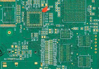
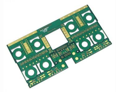
10-Layer Via-in-Pad Technology PCB features blind via in L9-10 in addition to the Fine Pitch BGA. Putting the via in the pad creates space on the external layers for more routing and avoids potential shorts during assembly. The routing channel widt
600V *RO4350B *RO4003C Dielectric material & Stack up requirement FR-4(no copper): 0.05-3.2mm for option Prepreg type: 7628H(7630), 7628(43%), 7628(41%), 2116HR, 2116, 2113, 1080 and 1060 for option Copper
Layer: 6 layers Material: FR-4 Board Thickness: 1.0mm Surface Finish:ENIG Copper Thickness: 1 oz all layers Blind via L1~L2 and L1~L3 Layers: 2--36layers Max manufacturing size: 640mm*1100mm Copper foil thickness: 0.5OZ-13OZ Min line width
Layer: 8 layers Material: FR-4 Board Thickness: 0.6mm Surface Finish: Immersion Gold 1~4u Copper Thickness: 1/3 oz Impedance, 4/4mils width/spacing Layers: 2--36layers Max manufacturing size: 640mm*1100mm Copper foil thickness: 0.5OZ-13OZ M
New Equipment | Design Services
Layer:4 Material:FR-4 4/4/4/4oz Thickness:2.0 Minimum hole:0.35mm Minimum Tracc/Spacing:12mil/15mil Application:power supply Layers: 2--36layers Max manufacturing size: 640mm*1100mm Copper foil thickness: 0.5OZ-13OZ Min line width/space:

Layer: 2 Material: FR-4 Board Thickness: 1.6mm Surface Finish: HAL Copper Thickness: 2/2 oz Green Solder Mask Layers: 2--36layers Max manufacturing size: 640mm*1100mm Copper foil thickness: 0.5OZ-13OZ Min line width/space: 3mil/3mil Min
Bicheng provides RD, high-tech, IT research companies and organizations, large or small with high quality bare PCB's PCB Products & Services * FR-4, High TG170, High CTI 600V * MCPCB, 1W/mk- 3W/mk * High speed

New Equipment | Assembly Services
Quick turn Prototype PCBs from 24 hour turnaround to high volume printed circuit board production from our domestic plant in USA and/or China facilities. Our Modern 38,000 sq. ft. manufacturing plant with multi-million dollar investment with latest e
Bicheng provides impedance controlled PCB's for R&D, high-tech, IT research companies and organizations, large or small. Technical parameters *Controlled dielectric *Controlled impedance *Design coupons *Test coupons *Po
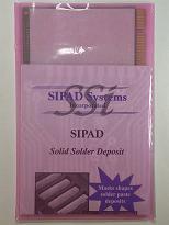
SIPAD Solid Solder Deposit (ssd) is a Siemens patented process that pre loads the pc board surface mount pads with solder in a solid form. Boards are printed, reflowed without components producing a predictable repeatable meniscus. SIPAD boards a

COT specializes in high quality SMT nozzles and consumables for pick and place machines. We provide special engineering design service of custom nozzles for those unique and odd components.
2481 Hilton Drive
Gainesville, GA USA
Phone: (770) 538-0411


