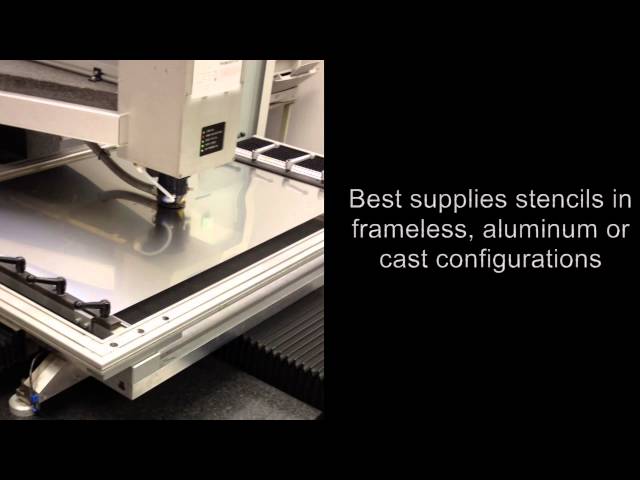
BEST manufactures and designs SMT stencils-both metal and plastic film type. This video demonstrates our metal stencil laser. See more on stencils here: http://www.soldertools.net/categories/Metal-Stencils/
BEST manufactures and designs SMT stencils-both metal and plastic film type. This video demonstrates our metal stencil laser. See more on stencils here: http://www.soldertools.net/categories/Metal-Stencils/
BEST manufactures and designs SMT stencils-both metal and plastic film type. This video demonstrates our metal stencil laser. See more on stencils here: http://www.soldertools.net/categories/Metal-Stencils/
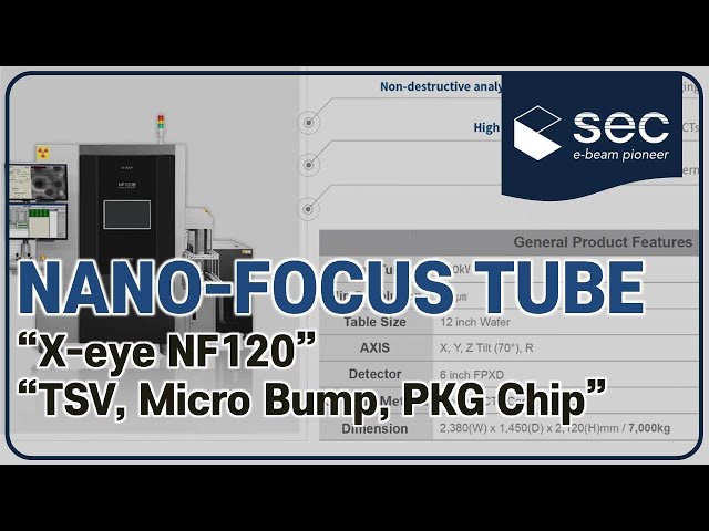
#Xray#Inspection#SEC Nano-focus Tube of 200 nano resolution which is specialized for sub-micron defects of Semiconductor Packaging, Wafer Level Packaging(WLP). -Non-destructive Analysis System -High-Resolution Image with Dual Type CTs -Application
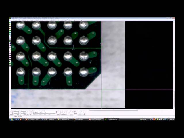
ScanCOMPONENT is a PC-based offline component programming system for the creation of vision data files from the smallest flip chip and bumped packages to the largest odd form devices. The ScanCOMPONENT is a standalone Product as well as a module of
| 1 |
.gif)


