DIP Double-side Camera Online AOI Machine ETA-V5300 If you could not find any similar items you want, you may send some photos to us. because our catalog and website haven't included all of our products. solder paste inspection,SMT SPI,SPI mac
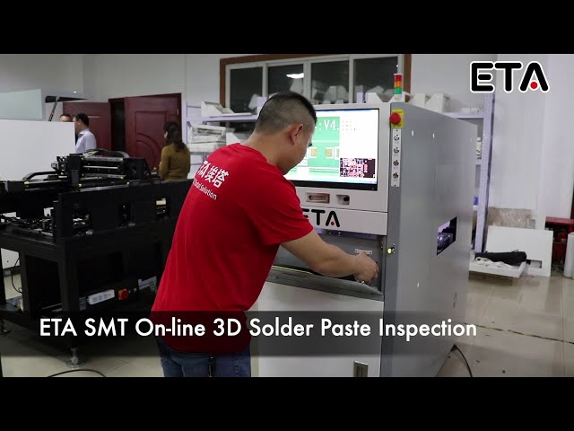
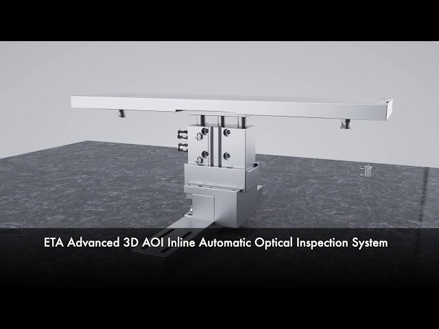
SMT On-line 3D Solder Paste Inspection If you could not find any similar items you want, you may send some photos to us. because our catalog and website haven't included all of our products. solder paste inspection,SMT SPI,SPI machine, SPI in

Inline 3D SPI, Standard Automatic solder paste inspection system As one of the strongest SMT 3D SPI Manufacuturer in China, we provide you all the different models of online solder paste inspection machine,we have variety of size and models of the
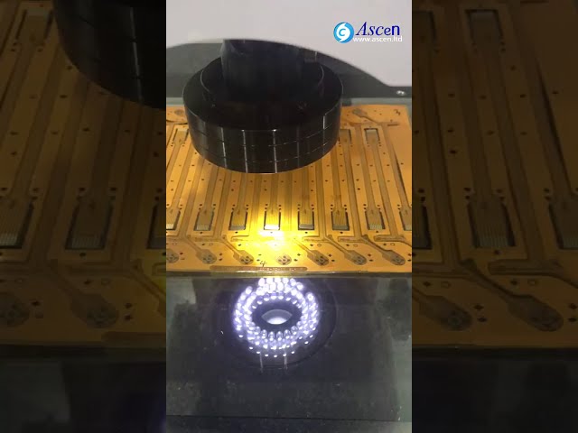
https://www.ascen.ltd/Products/PCB_board_assembly_system/vision_measurin/507.html Vision Measuring Machine and image measuring instrument can be used for dimensional accuracy measurement of various molds, aircraft, automobile, mobile phone, computer,
https://www.ascen.ltd/Products/PCB_board_assembly_system/vision_measurin/507.html Vision Measuring Machine and image measuring instrument can be used for dimensional accuracy measurement of various molds, aircraft, automobile, mobile phone, computer,
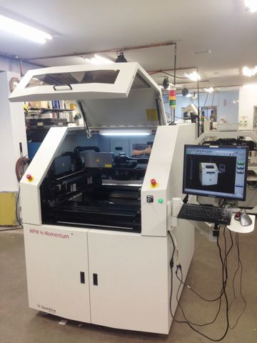
Description: FULLY AUTOMATIC SCREEN PRINTER Manufacturer: MPM Model: Momentum Plus (Speed Enhanced) Vintage: 9/8 / 2009 Condition: Reconditioned FEATURES: Windows 7 Operating System PCB Board Snuggers Edgeloc Momentum+Speed En
500,000 components per hour Maximum Board Size: 18” x 20” (457mm x 508mm) Clearance: 2” (50mm) top and bottom Minimum Component Size: 0201; 01005 with high magnification option
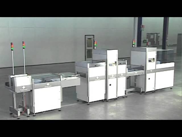
Successful manufacturing requires that the materials are in the right place Just on Time. Our board handling products are known for high quality, even our first PCB handling products from early 90’s are still used in many factories around the world.
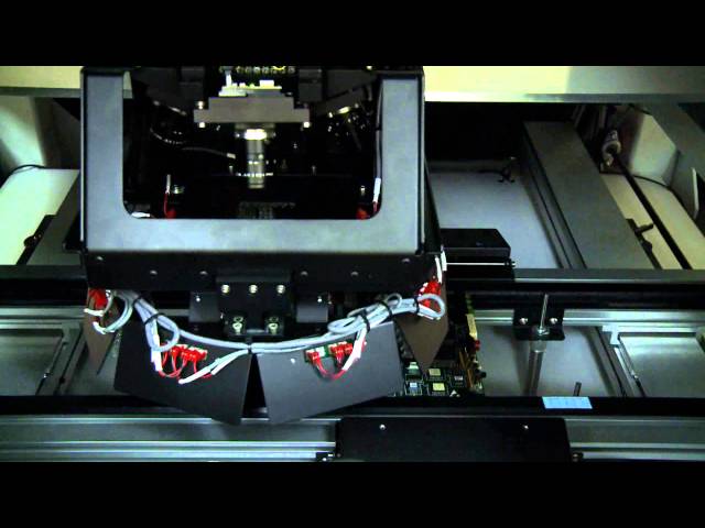
500,000 components per hour Maximum Board Size: 22” x 20” (560mm x 510mm) Clearance: 2” (50mm) top and bottom Minimum Component Size: 0201; 01005 with high magnification option
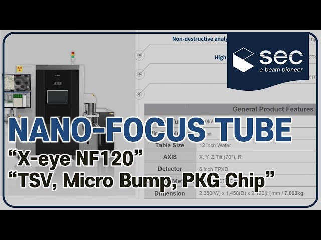
#Xray#Inspection#SEC Nano-focus Tube of 200 nano resolution which is specialized for sub-micron defects of Semiconductor Packaging, Wafer Level Packaging(WLP). -Non-destructive Analysis System -High-Resolution Image with Dual Type CTs -Application


