iNEMI is an industry-led consortium focused on identifying and closing technology gaps, which includes the development and integration of the electronics industry supply infrastructure.
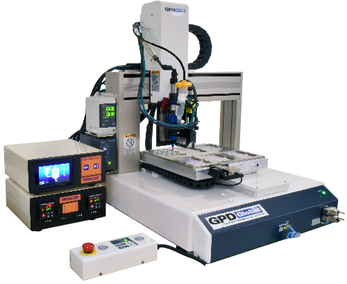
Full-featured and compact benchtop dispense system robot offering accurate and repeatable dispense results! A benchtop dispense system does not mean "no features". The Catalina benchtop dispense system is a full-featured platform with these standard

New Equipment | Solder Paste Stencils
MPM UP2000 HiE Screen Printer Substrate treatment Minimum/maximum size 2"x 2"(50.0 mm x50.0 mm) to 20" x 16" (508 mm x 406 mm)(16 "or larger substrate requires special clamps
Electronics Forum | Mon Sep 18 11:55:35 EDT 2000 | Ricardo Fuentes
Hi! cold someone advise me about the minimum gap allowable in between 0404 parts. The minimum distance is because of the behavior on reflow, the re-work difficulty or anything else. Thanks
Electronics Forum | Thu Jun 25 05:19:39 EDT 2020 | SMTA-Davandran
Dear all, Anyone know what is minimum gap between SMT component.? Anyone have design guideline for it.
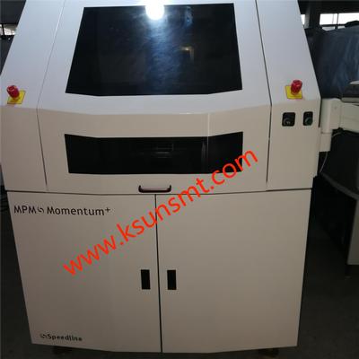
Used SMT Equipment | Screen Printers
MPM Momentum+ Printer Substrate treatment Maximum plate size(XxY) 609.6 mm x 508 mm(24”x 20”) Segmented mode-Momentum Elite 457 mm x 508 mm(18"x20") Minimum Plate Size (XxY)
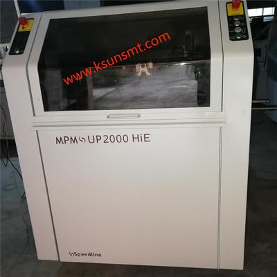
Used SMT Equipment | Screen Printers
MPM UP2000HiE PRINTER Substrate treatment Minimum/maximum size 2"x 2"(50.0 mm x50.0 mm) to 20" x 16" (508 mm x 406 mm)(16 "or larger substrate requires special clamps) Thickness rang
Industry News | 2003-02-19 08:39:25.0
GSPK Circuits is Taking Courageous Steps to Bridge the Missing "complete supply solution" Service Gap to Benefit Its Customers by Investing in a Brand New Chinese Venture
Industry News | 2003-05-02 08:49:07.0
Group to Assemble Data by Package and Technology Type
Parts & Supplies | Pick and Place/Feeders
CLAMPING GAP X-BELT S25 HM2
Technical Library | 2024-03-19 15:53:34.0
Underfill is a composite material usually made of an epoxy polymer that fills gaps between a chip and its carrier or a finished package and the PCB substrate to connect the chip to the board.
Technical Library | 2021-09-02 08:17:07.0
We are a professional manufacturer of PCB depaneling machines, which is workable for all boards, including flex and regid boards, v-scored boards and routed boards. Laser pcb depaneling is non-contact way without mechanical stress,this solution is good for modern precision PCB depaneling. It has below advantages: 1. No dust The production environment of the circuit board industry is carried out in the dust-free workshop. The traditional pcb depaneling equipment, such as blade moving type machine, will inevitably produce residues and micro powder, which will pollute the 10000 and 1000 class dust-free workshops and affect the conductivity of products. The UV laser PCB cutting machine is a vaporization processing process, which will not produce dust and is conducive to the conductivity of the product. 2. High cutting precision The processing gap of high-precision traditional processing equipment can not reach the gap width of less than 100 microns, which will cause certain damage to the lines on the edge or PCBA circuit board containing components. The focus spot of the laser cutting machine is small, and the ultraviolet cold processing mode has little thermal impact on the edge of the circuit board. The cutting position accuracy is less than 50 microns, and the cutting size accuracy is less than 30 microns, which will not affect the edge of the circuit board, and the precision is high. 3. No stress Traditional processing methods generally have V-grooves, which will cause certain damage to the board in the manufacturing process. The UV laser PCB cutting machine can directly cut the bare board without making V-grooves. In addition, the traditional processing methods directly use tools to act on the circuit board, especially the stamping method has a great impact on the circuit board, which is easy to cause board deformation. The laser cutting machine is a non-contact processing mode, which acts on the surface of the material through the high-energy beam, which will not cause the influence of stress and the deformation and damage of the circuit board. 4. For special-shaped cutting, it is easy to automate The UV laser PCB cutting machine can cut for any shape without replacing any props and fixtures, and without steel mesh. The same equipment can meet special-shaped and straight-line cutting, which is easy to realize assembly line automatic production and high flexibility. It is easy to improve production efficiency and save production process and production cycle. In particular, it can quickly and efficiently meet the needs of rapid proofing, directly import the drawing, and then locate the cutting. 5. High compatibility The UV laser PCB cutting machine can process the materials around the circuit board, such as PCB, FPC, covering film, pet, reinforcing board, IC, ultra-thin metal cutting, etc. it has strong practicability, is compatible with the processing of a variety of materials, is easy to operate, can be imported into the drawing, does not need to adjust any mechanical parts, and is easy to operate and maintain. 6. Good cutting edge effect The cutting edge is smooth and neat without burr. It can be processed and formed directly according to the size of the drawing, which is conducive to improving the yield of the product. It can be directly installed into the subsequent process without further processing. For more details about UV laser depaneling, please feel free to contact us. www.pcbdepanelingrouter.com

FKN Systek K3000 - Singulate scored and skip scored panels up to 24" long ESD protective mat on back table Adjustable front and back support table Singulate panels with components up to 2.5" high Available in 18" blade (standard) or 24" blade (
Training Courses | ON DEMAND | | PCB Design Courses
The PCB design courses teach students the process, techniques and tools needed to design layout of printed circuit boards.
Training Courses | ON DEMAND | | PCB Design Courses
The PCB design courses teach students the process, techniques and tools needed to design layout of printed circuit boards.
Events Calendar | Sun Sep 27 00:00:00 EDT 2020 - Thu Oct 01 00:00:00 EDT 2020 | Rosemont, Illinois USA
SMTA International 2020 Conference & Exhibition
Events Calendar | Wed Dec 01 00:00:00 EST 2021 - Wed Dec 01 00:00:00 EST 2021 | ,
Wine Down Wednesday: Driving Innovation through Intrapreneurship
Career Center | Altoona, Pennsylvania USA | Sales/Marketing
MacDermid Alpha Electronics Solutions, a Element Solutions, Inc. business and world leader in the development, manufacturing, and sales of innovative materials used in the assembly electronics, industrial joining and Photo Voltaic market places, is s
Career Center | , India | Engineering,Production
About Product Operations: Product Operations is part of Global Supply Chain Management (Global Manufacturing) and is responsible for New Product Introduction and Product Life Cycle Management from Manufacturing and Supply Operations perspective. The
Career Center | Noida, India | Maintenance,Management,Production
Over 12 years of experience in Assembly Line Production, PCB, SMT, Process Improvements, testing & troubleshooting, time and motion study, Value– Engineering as well as Quality in varied industries.
Career Center | Noida, India | Maintenance,Production
Over 12 years of experience in Assembly Line Production, PCB, SMT, Process Improvements, testing & troubleshooting, time and motion study, Value– Engineering as well as Quality in varied industries.
SMTnet Express, November 7, 2019, Subscribers: 32,325, Companies: 10,919, Users: 25,284 Origin and Quantification of Increased Core Loss in MnZn Ferrite Plates of a Multi-Gap Inductor Credits: Power Electronic Systems Laboratory (PES) Inductors


