Electronics Manufacturing Technical Articles
Papers and articles related to SMT, PCB & EMS industry.
- SMTnet
- »
- Technical Library

1857 SMT / PCB Assembly Related Technical Articles
Hebrew University of Jerusalem
Israel's second-oldest university, the Hebrew University is the top university in Israel, overall the 59th-best university in the world.
Jerusalem, Israel
The University of Baghdad (UOB) is the largest university in Iraq and the second largest Arab university.
Baghdad, Iraq
Hubei University of Technology
With a history of over 50 years, Hubei University of Technology (HBUT) is a provincial multi-discipline university, specializing in engineering.
Wuhan, China
At Tridonic our daily quest is to create perfect light. 2,000 experts worldwide are working tirelessly to control, regulate and operate lighting in exactly the way you want it. And we have been doing this for more than 50 years.
Dornbirn, Austria

One of the world's leading suppliers of integrated production systems, chemistry, equipment, know-how and service for electroplating, semiconductor and printed circuit board manufacturing.
Berlin, Germany
Universal Instruments Corporation
Universal Instruments is a global leader in the design and manufacture of advanced automation and assembly equipment solutions for the electronics manufacturing industry.
Conklin, New York, USA
Schleuniger, Inc. is a leading manufacturer of wire processing equipment. Our innovative automatic and semi-automatic machines are designed to cut, strip, crimp and mark all types of wire and cable.
Manchester, New Hampshire, USA
A leading supplier of precision cleaning chemistries to the worldwide electronics, metal finishing, medical, semiconductor, and optical industries.
Nashville, Tennessee, USA
Freescale is a leader in embedded processing solutions. From microcontrollers and microprocessors to sensors, analog ICs and connectivity, our technologies are fueling the next great wave of innovation.
Austin, Texas, USA
Kolb Cleaning Technology USA LLC
The international full service manufacturer of systems, detergents, equipment and process design for the cleaning in electronics production.
Longmont, Colorado, USA
Flex (Flextronics International)
Flextronics is a global full-service supplier of a full spectrum of value-added Electronic Manufacturing Services.
Singapore, Singapore
Cree is a market leader in LED chips, power LEDs, LED backlighting, power switching and wireless communications devices.
Durham, North Carolina, USA
AT&S is currently Europe’s largest printed circuit board manufacturer and one of the market leaders in high-end printed circuit board technology.
Leoben, Austria
BEST offers professional rework, repair and prototype builds of PCBs. Our expertise is on BGA rework and QFN rework. Our experienced instructors teach professional soldering classes as we are an IPC certified training center
Rolling Meadows, Illinois, USA
BEST offers professional rework, repair and prototype builds of PCBs. Our expertise is on BGA rework and QFN rework. Our experienced instructors teach professional soldering classes as we are an IPC certified training center
Rolling Meadows, Illinois, USA
BEST offers professional rework, repair and prototype builds of PCBs. Our expertise is on BGA rework and QFN rework. Our experienced instructors teach professional soldering classes as we are an IPC certified training center
Rolling Meadows, Illinois, USA
Honeywell is a Fortune 100 company that invents and manufactures technologies to address tough challenges linked to global macrotrends such as safety, security, and energy.
Morristown, New Jersey, USA
DfR Solutions (acquired by ANSYS Inc)
DfR Solutions has world-renowned expertise in applying the science of Reliability Physics to electrical and electronics technologies, and is a leading provider of quality, reliability, and durability (QRD) research and consulting
College Park,

Leading provider of full-field metrology solutions for substrates and packages in the OEM/CEM/SATS/PCB segments of the microelectronics industry.
Atlanta, Georgia, USA
Leading provider of full-field metrology solutions for substrates and packages in the OEM/CEM/SATS/PCB segments of the microelectronics industry.
Atlanta, Georgia, USA
Leading provider of full-field metrology solutions for substrates and packages in the OEM/CEM/SATS/PCB segments of the microelectronics industry.
Atlanta, Georgia, USA
A world leader in high-performance PCB fabrication & assembly, semiconductor packaging, systems integration & test, advanced laboratory services and contract R&D.
Endicott, New York, USA
DfR Solutions (acquired by ANSYS Inc)
DfR Solutions has world-renowned expertise in applying the science of Reliability Physics to electrical and electronics technologies, and is a leading provider of quality, reliability, and durability (QRD) research and consulting
College Park,
The UT is one of the 14 state universities in Ohio offering over 250 academic programs in a diverse and comprehensive range of studies
Toledo, Ohio, USA
DfR Solutions (acquired by ANSYS Inc)
DfR Solutions has world-renowned expertise in applying the science of Reliability Physics to electrical and electronics technologies, and is a leading provider of quality, reliability, and durability (QRD) research and consulting
College Park,
A premier thermal management solutions company. Our highly engineered products include Heat Pipes, Heat Exchangers and Cold Plates.
Lancaster, Pennsylvania, USA
A research university located in Beijing, China, and one of the nine members in the C9 League.
Beijing, China
Nepes offers flip chip solutions ranging from wafer bumping to advanced packaging and testing for IC manufactures, module electronics and end-product makers.
Seoul, South Korea
Cisco designs, manufactures, and sells Internet protocol (IP)-based networking and other products related to the communications and IT industry and provide services associated with these products.
San Jose, CA, USA
For everything from high volume, low cost capacitors to application specific ceramic solutions, Johanson Dielectrics has you covered.
Sylmar, California, USA
National Chiao Tung University
NCTU is one of the oldest and most prestigious universities in Taiwan,
Hsinchu City, Taiwan
WASET - World Academy of Science, Engineering and Technology
A scholarly open access, peer-reviewed, interdisciplinary, monthly and fully refereed journal focusing on theories, methods and applications in Science, Engineering and Technology.
Riverside, Connecticut, USA
A leading supplier of precision cleaning chemistries to the worldwide electronics, metal finishing, medical, semiconductor, and optical industries.
Nashville, Tennessee, USA
YINCAE Advanced Materials, LLC.
Yincae Advanced Materials, LLC is a developer, manufacturer, and supplier of high performance coatings, adhesives, electronic and optoelectronic materials.
Albany, New York, USA
Institute of Electrical and Electronics Engineers (IEEE)
IEEE is the world's largest professional association dedicated to advancing technological innovation and excellence for the benefit of humanity.
Piscataway, New Jersey, USA
Mohammed V University at Agdal offers a wide set of degrees both in the undergraduate and graduate levels.
Rabat, Morocco
USM offers courses ranging from Natural Sciences, Applied Sciences, Medical and Health Sciences, Pharmaceutical Sciences to Building Science and Technology, Social Sciences, Humanities, and Education.
Pulau, Penang, Malaysia

AIM is a leading global manufacturer of solder assembly materials for the electronics industry.
Montreal, Quebec, Canada
YINCAE Advanced Materials, LLC.
Yincae Advanced Materials, LLC is a developer, manufacturer, and supplier of high performance coatings, adhesives, electronic and optoelectronic materials.
Albany, New York, USA
The Die Products Consortium (DPC) is a group of leading microelectronic companies collaborating to expand the market for semiconductor die products.
Austin, Texas, USA
Cornell University's colleges, schools, and other academic units offer more than 4,000 courses, 70 undergraduate majors, 93 graduate fields of study, undergraduate and advanced degrees.
Ithaca, New York, USA
RSN champions human rights with vulnerable communities in the mining and harvesting of raw materials found in products we use every day.
Oakland, California, USA
YINCAE Advanced Materials, LLC.
Yincae Advanced Materials, LLC is a developer, manufacturer, and supplier of high performance coatings, adhesives, electronic and optoelectronic materials.
Albany, New York, USA
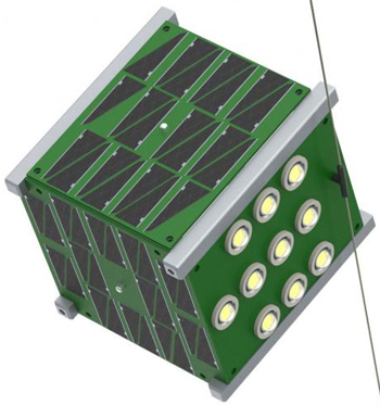
We are a student group at Brown University working to build a low-cost, open-source CubeSat, EQUiSat.
Providence, Rhode Island, USA
Institute of Electrical and Electronics Engineers (IEEE)
IEEE is the world's largest professional association dedicated to advancing technological innovation and excellence for the benefit of humanity.
Piscataway, New Jersey, USA
Inventec Performance Chemicals
Inventec, one of Europe's leading Performance Chemicals companies, is the high-tech industries business of the Dehon Group
Vincennes , France

Leading materials science company that provides high performance materials, chemistry and technology solutions to the electronics and surface finishing industries worldwide.
Lakeville, Minnesota, USA
Just Connectors - Supplier of high-grade connectors and interconnects parts
Anaheim, California, USA
Manufacturer of vapor phase soldering systems and associated products since 1985.
Königsbrunn, Germany
Budapest University of Technology and Economics
BME is considered the world's oldest Institute of Technology which has university rank and structure. It was the first institute in Europe to train engineers at university level.
Budapest, Hungary


.gif)