Electronics Manufacturing Technical Articles

Electronics Manufacturing Technical Articles

Papers and articles related to SMT, PCB & EMS industry.


  • Reflow Ovens
  • Precision, fluid dispensing systems for low volume, high mix, R&D, and high volume 24x7 production

Add Article »

1882 SMT / PCB Assembly Related Technical Articles

Solder Joint Reliability Under Realistic Service Conditions

Oct 30, 2014 | P. Borgesen, S. Hamasha, M. Obaidat, V. Raghavan, X. Dai; Department of Systems Science & Industrial Engineering, Binghamton University, M. Meilunas, M. Anselm; Universal Instruments Corporation.

The ultimate life of a microelectronics component is often limited by failure of a solder joint due to crack growth through the laminate under a contact pad (cratering), through the intermetallic bond to the pad, or through the solder itself. Whatever the failure mode proper assessments or even relative comparisons of life in service are not possible based on accelerated testing with fixed amplitudes, or random vibration testing, alone. Effects of thermal cycling enhanced precipitate coarsening on the deformation properties can be accounted for by microstructurally adaptive constitutive relations, but separate effects on the rate of recrystallization lead to a break-down in common damage accumulation laws such as Miner's rule. Isothermal cycling of individual solder joints revealed additional effects of amplitude variations on the deformation properties that cannot currently be accounted for directly.

We propose a practical modification to Miner's rule for solder failure to circumvent this problem. Testing of individual solder pads, eliminating effects of the solder properties, still showed variations in cycling amplitude to systematically reduce subsequent acceleration factors for solder pad cratering. General trends, anticipated consequences and remaining research needs are discussed...

Publisher: Universal Instruments Corporation

Universal Instruments Corporation

Universal Instruments is a global leader in the design and manufacture of advanced automation and assembly equipment solutions for the electronics manufacturing industry.

Conklin, New York, USA

Manufacturer

5 Questions to Ask Before Choosing a New Cut and Strip Machine

Oct 27, 2014 | Pete Doyon, VP Product Management, Schleuniger, Inc.

A lot of time and effort often goes into finding the right equipment for your facility. Purchasing a new wire cut & strip machine is no different. With so many options, where does one start? Asking these five questions during the decision making process will help ensure you end up with equipment that fits all of your needs. ...

Publisher: Schleuniger, Inc.

Schleuniger, Inc.

Schleuniger, Inc. is a leading manufacturer of wire processing equipment. Our innovative automatic and semi-automatic machines are designed to cut, strip, crimp and mark all types of wire and cable.

Manchester, New Hampshire, USA

Other

Combination of Spray and Soak Improves Cleaning under Bottom Terminations

Oct 23, 2014 | Dr. Mike Bixenman; Kyzen Corporation, Julie Fields; Technical Devices Company, Eric Camden; Foresite.

The functional reliability of electronic circuits determines the overall reliability of the product in which the final products are used. Market forces including more functionality in smaller components, no-clean lead-free solder technologies, competitive forces and automated assembly create process challenges. Cleanliness under the bottom terminations must be maintained in harsh environments. Residues under components can attract moisture and lead to leakage currents and the potential for electrochemical migration (...)

The purpose of this research study is to evaluate innovative spray and soak methods for removing low residue flux residues and thoroughly rinsing under Bottom Termination and Leadless Components...

Publisher: KYZEN Corporation

KYZEN Corporation

A leading supplier of precision cleaning chemistries to the worldwide electronics, metal finishing, medical, semiconductor, and optical industries.

Nashville, Tennessee, USA

Manufacturer

Oxide Thickness and Solderability Methodology to Determine Long Term Storage of BGAs and QFPs

Oct 16, 2014 | Rama Hegde, senior member of technical staff; Freescale Semiconductor.

Key points are:

*Long-term storage of BGA & QFP products may be required due to:

  • Fab and assembly factory transfers
  • Product obsolescence requiring customers make lifetime/EOL purchases
  • Providing extended service (10+ years) on vehicles
  • Other program needs
  • * Integrity of EOL products in terms of solderability needs to be verified....

    Publisher: Freescale Semiconductor Inc

Freescale Semiconductor Inc

Freescale is a leader in embedded processing solutions. From microcontrollers and microprocessors to sensors, analog ICs and connectivity, our technologies are fueling the next great wave of innovation.

Austin, Texas, USA
Manufacturer

Cleaning Of Assembled PCBs - A Crucial Way of Enhancing Product Reliability and Avoiding Problems in the Field

Oct 09, 2014 | Wilfried Clemens.

Over the last years more and more international newspapers reported in Europe / USA and Japan: "Tunnel train got stuck under the Channel – thousands of people stranded", "Recall of thousands of cars to workshops for control and repair", "Power Failures left households without energy for hours." Very often news like this relate to malfunctions of electric and electronic circuits under adverse conditions or sometimes even in normal operating environment (...)

The presentation will deal with all kinds of aspect of cleaning to ensure the reliability of electronic circuitry in ever changing operation conditions in the most important industrial areas....

Publisher: Kolb Cleaning Technology USA LLC

Kolb Cleaning Technology USA LLC

The international full service manufacturer of systems, detergents, equipment and process design for the cleaning in electronics production.

Longmont, Colorado, USA

Manufacturer

Assembly Process Feasibility of Low/No Silver Alloy Solder Paste Materials

Oct 02, 2014 | Jennifer Nguyen Ranilo Aranda, David Geiger, and Murad Kurwa

Sn3.0Ag0.5Cu (SAC305) is the most popular near eutectic lead-free alloy used in the manufacturing processes. Over the last several years, the price of silver has dramatically increased driving a desire for lower silver alloy alternatives. As the results, there is a significant increase in the number of alternative low/no silver lead-free solder alloys available in the industry recently.

In this paper, we'll present the performance and process capability of various low/no silver alloy solder pastes. Data from printability, wetting test, slump test, solder ball test, voiding, etc… will be discussed and compared with the control SAC305 solder paste. Benefits and concerns of using low/no silver alloy solder paste materials will also be addressed....

Publisher: Flex (Flextronics International)

Flex (Flextronics International)

Flextronics is a global full-service supplier of a full spectrum of value-added Electronic Manufacturing Services.

Singapore, Singapore

Consultant / Service Provider

Taking the LED Pick and Place Challenge

Sep 25, 2014 | Joshua J. Markle.

For the past few years there has been a shift in the Lighting Industry that has carried over to the surface mount technology assembly line. What is this shift you may ask? Well it is the LED revolution. This revolution or change in lighting has some very promising results already in practice and many more companies looking to implement the LED technology into their product portfolio's. With a number of companies looking to expand their portfolio to include LED fixtures there has been an increase in the number of companies that have started their own SMT lines, as well as a significant number of contract manufacturers to meet this new industries demands (...)

This presentation will discuss some issues in the pick and place process for LEDs and presents a method to troubleshoot and resolve these issues....

Publisher: Cree, Inc.

Cree, Inc.

Cree is a market leader in LED chips, power LEDs, LED backlighting, power switching and wireless communications devices.

Durham, North Carolina, USA

Manufacturer's Representative

Predicting the Lifetime of the PCB - From Experiment to Simulation

Sep 18, 2014 | Markus Leitgeb, AT&S Peter Fuchs, PCCL.

Two major drivers in electronic industry are electrical and mechanical miniaturization. Both induce major changes in the material selection as well as in the design. Nevertheless, the mechanical and thermal reliability of a Printed Circuit Board (PCB) has to remain at the same high level or even increase (e.g. multiple lead-free soldering). To achieve these reliability targets, extensive testing has to be done with bare PCB as well as assembled PCB. These tests are time consuming and cost intensive. The PCBs have to be produced, assembled, tested and finally a detailed failure analysis is required to be performed.

This paper examines the development of our concept and has the potential to enable the prediction of the lifetime of the PCB using accelerated testing methods and finite element simulations....

Publisher: AT&S

AT&S

AT&S is currently Europe’s largest printed circuit board manufacturer and one of the market leaders in high-end printed circuit board technology.

Leoben, Austria

Manufacturer

Plastic vs Metal Stencils for Prototype Printing

Sep 11, 2014 | Bob Wettermann.

This article goes through the pluses and minuses of using plastic stencils for DIY prototypes. The release efficiency is measured and "rules of thumb" for using one type vs another is explained....

Publisher: BEST Inc.

BEST Inc.

BEST offers professional rework, repair and prototype builds of PCBs. Our expertise is on BGA rework and QFN rework. Our experienced instructors teach professional soldering classes as we are an IPC certified training center

Rolling Meadows, Illinois, USA

Consultant / Service Provider, Manufacturer

Reliability of Reworked QFNs

Sep 11, 2014 | CRANE.

In this DOD study the reliability of reworked QFNs is studied with the outcome being that a stay in place stencil does not impact the reliability of a QFN reworked using this technique...

Publisher: BEST Inc.

BEST Inc.

BEST offers professional rework, repair and prototype builds of PCBs. Our expertise is on BGA rework and QFN rework. Our experienced instructors teach professional soldering classes as we are an IPC certified training center

Rolling Meadows, Illinois, USA

Consultant / Service Provider, Manufacturer

Reballing a QFN Simplifies QFN Rework

Sep 11, 2014 | Bob Wettermann.

There are a variety of methods one can use to rework QFNs. This paper explains one of the ways to get very little center ground voiding while making it easy to place a tiny component with almost no keep out areas....

Publisher: BEST Inc.

BEST Inc.

BEST offers professional rework, repair and prototype builds of PCBs. Our expertise is on BGA rework and QFN rework. Our experienced instructors teach professional soldering classes as we are an IPC certified training center

Rolling Meadows, Illinois, USA

Consultant / Service Provider, Manufacturer

Counterfeit Integrated Circuits: Detection, Avoidance, and the Challenges Ahead.

Sep 04, 2014 | U. Guin, M. Tehranipoor - ECE Department, University of Connecticut, D. DiMase - Honeywell Inc.,

The counterfeiting of electronic components has become a major challenge in the 21st century. The electronic component supply chain has been greatly affected by widespread counterfeit incidents. A specialized service of testing, detection, and avoidance must be created to tackle the worldwide outbreak of counterfeit integrated circuits (ICs). So far, there are standards and programs in place for outlining the testing, documenting, and reporting procedures. However, there is not yet enough research addressing the detection and avoidance of such counterfeit parts.

In this paper we will present, in detail, all types of counterfeits, the defects present in them, and their detection methods. We will then describe the challenges to implementing these test methods and to their effectiveness. We will present several anti-counterfeit measures to prevent this widespread counterfeiting, and we also consider the effectiveness and limitations of these anti-counterfeiting techniques....

Publisher: Honeywell International

Honeywell International

Honeywell is a Fortune 100 company that invents and manufactures technologies to address tough challenges linked to global macrotrends such as safety, security, and energy.

Morristown, New Jersey, USA

Manufacturer

The Effect of Coating and Potting on the Reliability of QFN Devices.

Aug 28, 2014 | Greg Caswell, Cheryl Tulkoff.

The fastest growing package types in the electronics industry today are Bottom Termination Components (BTCs). While the advantages of BTCs are well documented, they pose significant reliability challenges to users. One of the most common drivers for reliability failures is the inappropriate adoption of new technologies. This is especially true for new component packaging like BTCs. Obtaining relevant information can be difficult since information is often segmented and the focus is on design opportunities not on reliability risks (...)

Commonly used conformal coating and potting processes have resulted in shortened fatigue life under thermal cycling conditions. Why do conformal coating and potting reduce fatigue life? This paper details work undertaken to understand the mechanisms underlying this reduction. Verification and determination of mechanical properties of some common materials are performed and highlighted. Recommendations for material selection and housing design are also given....

Publisher: DfR Solutions (acquired by ANSYS Inc)

DfR Solutions (acquired by ANSYS Inc)

DfR Solutions has world-renowned expertise in applying the science of Reliability Physics to electrical and electronics technologies, and is a leading provider of quality, reliability, and durability (QRD) research and consulting

College Park,

Consultant / Service Provider

Implementing Warpage Management: A Five-Step Process for EMS Providers

Aug 19, 2014 | Ken Chiavone

Warpage management consists of planning, measuring, analyzing, sharing, and reacting to data related to the surface shapes of electronics components as they change throughout the reflow assembly process. Leading semiconductor manufacturers have had warpage management systems in place for ten years or more, mainly because microchip package warpage must be understood and compensated for in order to attain high assembly yields. Similarly, newer device architectures such as package-on-package and system-on-a-chip are sensitive to warpage-related assembly issues, and companies involved in the manufacture and assembly of these devices tend to have the most advanced warpage management programs....

Publisher: Akrometrix

Akrometrix

Leading provider of full-field metrology solutions for substrates and packages in the OEM/CEM/SATS/PCB segments of the microelectronics industry.

Atlanta, Georgia, USA

Consultant / Service Provider, Manufacturer

Advanced Second Level Assembly Analysis Techniques - Troubleshooting Head-In-Pillow, Opens, and Shorts with Dual Full-Field 3D Surface Warpage Data Sets/

Aug 19, 2014 | Ken Chiavone

SMT assembly planning and failure analysis of surface mount assembly defects often include component warpage evaluation. Coplanarity values of Integrated Circuit packages have traditionally been used to establish pass/fail limits. As surface mount components become smaller, with denser interconnect arrays, and processes such package-on-package assembly become prevalent, advanced methods using dual surface full-field data become critical for effective Assembly Planning, Quality Assurance, and Failure Analysis. A more complete approach than just measuring the coplanarity of the package is needed. Analyzing the gap between two surfaces that are constantly changing during the reflow thermal cycle is required, to effectively address the challenges of modern SMT assembly....

Publisher: Akrometrix

Akrometrix

Leading provider of full-field metrology solutions for substrates and packages in the OEM/CEM/SATS/PCB segments of the microelectronics industry.

Atlanta, Georgia, USA

Consultant / Service Provider, Manufacturer

Ready to Start Measuring PCB Warpage during Reflow? Why and How to Use the New IPC-9641 Standard

Aug 19, 2014 | Ken Chiavone

Understanding warpage of package attach locations on PCBs under reflow temperature conditions is critical in surface mount technology. A new industry standard, IPC 9641, addresses this topic directly for the first time as an international standard.

This paper begins by summarizing the sections of the IPC 9641 standard, including, measurement equipment selection, test setup and methodology, and accuracy verification. The paper goes further to discuss practical implementation of the IPC 9641 standards. Key advantages and disadvantages between available warpage measurement methods are highlighted. Choosing the correct measurement technique depends on requirements for warpage resolution, data density, measurement volume, and data correlation. From industry experience, best practice recommendations are made on warpage management of PCB land areas, covering how to setup, run, analyze, and report on local area PCB warpage.

The release of IPC 9641 shows that flatness over temperature of the package land area on the PCB is critical to the SMT industry. Furthermore, compatibility of shapes between attaching surfaces in SMT, like a package and PCB, will be critical to product yield and quality in years to come....

Publisher: Akrometrix

Akrometrix

Leading provider of full-field metrology solutions for substrates and packages in the OEM/CEM/SATS/PCB segments of the microelectronics industry.

Atlanta, Georgia, USA

Consultant / Service Provider, Manufacturer

Advanced Organic Substrate Technologies To Enable Extreme Electronics Miniaturization.

Aug 14, 2014 | Susan Bagen, Dave Alcoe, Kim Blackwell, Frank Egitto.

High reliability applications for high performance computing, military, medical and industrial applications are driving electronics packaging advancements toward increased functionality with decreasing degrees of size, weight and power (SWaP) The substrate technology selected for the electronics package is a key enabling technology towards achieving SWaP. Standard printed circuit boards (PWBs) utilize dielectric materials containing glass cloth, which can limit circuit density and performance, as well as inhibit the ability to achieve reliable assemblies with bare semiconductor die components. Ceramic substrates often used in lieu of PWBs for chip packaging have disadvantages of weight, marginal electrical performance and reliability as compared to organic technologies. Alternative materials including thin, particle-containing organic substrates, liquid crystal polymer (LCP) and microflex enable SWaP, while overcoming the limitations of PWBs and ceramic.

This paper will discuss the use of these alternative organic substrate materials to achieve extreme electronics miniaturization with outstanding electrical performance and high reliability. The effect of substrate type on chip-package interaction and resulting reliability will be discussed. Microflex assemblies to achieve extreme miniaturization and atypical form factors driven by implantable and in vivo medical applications are also shown....

Publisher: i3 Electronics

i3 Electronics

A world leader in high-performance PCB fabrication & assembly, semiconductor packaging, systems integration & test, advanced laboratory services and contract R&D.

Endicott, New York, USA

Manufacturer

Gold Embrittlement In Lead-Free Solder.

Aug 07, 2014 | Craig Hillman, Nathan Blattau, Joelle Arnold, Thomas Johnston, Stephanie Gulbrandsen; DfR Solutions, Julie Silk, Alex Chiu; Agilent Technologies.

Gold embrittlement in SnPb solder is a well-known failure mechanism in electronic assembly. To avoid this issue, prior studies have indicated a maximum gold content of three weight percent. This study attempts to provide similar guidance for Pb-free (SAC305) solder. Standard surface mount devices were assembled with SnPb and SAC305 solder onto printed boards with various thicknesses of gold plating. The gold plating included electroless nickel immersion gold (ENIG) and electrolytic gold of 15, 25, 35, and 50 microinches over nickel. These gold thicknesses resulted in weight percentages between 0.4 to 7.0 weight percent....

Publisher: DfR Solutions (acquired by ANSYS Inc)

DfR Solutions (acquired by ANSYS Inc)

DfR Solutions has world-renowned expertise in applying the science of Reliability Physics to electrical and electronics technologies, and is a leading provider of quality, reliability, and durability (QRD) research and consulting

College Park,

Consultant / Service Provider

Electrostatic Theory of Metal Whiskers.

Jul 31, 2014 | V. G. Karpov, Department of Physics and Astronomy, University of Toledo.

Metal whiskers often grow across leads of electric equipment and electronic package causing current leakage or short circuits and raising significant reliability issues. The nature of metal whiskers remains a mystery after several decades of research. Here, the existence of metal whiskers is attributed to the energy gain due to electrostatic polarization of metal filaments in the electric field. The field is induced by surface imperfections: contaminations, oxide states, grain boundaries, etc. A proposed theory provides closed form expressions and quantitative estimates for the whisker nucleation and growth rates, explains the range of whisker parameters and effects of external biasing, and predicts statistical distribution of their lengths....

Publisher: University of Toledo

University of Toledo

The UT is one of the 14 state universities in Ohio offering over 250 academic programs in a diverse and comprehensive range of studies

Toledo, Ohio, USA

Research Institute / Laboratory / School

Copper Wire Bond Failure Mechanisms.

Jul 24, 2014 | Randy Schueller, Ph.D.

Wire bonding a die to a package has traditionally been performed using either aluminum or gold wire. Gold wire provides the ability to use a ball and stitch process. This technique provides more control over loop height and bond placement. The drawback has been the increasing cost of the gold wire. Lower cost Al wire has been used for wedge-wedge bonds but these are not as versatile for complex package assembly. The use of copper wire for ball-stitch bonding has been proposed and recently implemented in high volume to solve the cost issues with gold. As one would expect, bonding with copper is not as forgiving as with gold mainly due to oxide growth and hardness differences.

This paper will examine the common failure mechanisms that one might experience when implementing this new technology....

Publisher: DfR Solutions (acquired by ANSYS Inc)

DfR Solutions (acquired by ANSYS Inc)

DfR Solutions has world-renowned expertise in applying the science of Reliability Physics to electrical and electronics technologies, and is a leading provider of quality, reliability, and durability (QRD) research and consulting

College Park,

Consultant / Service Provider

Enhancing Thermal Performance in Embedded Computing for Ruggedized Military and Avionics Applications.

Jul 17, 2014 | Darren Campo, Jens Weyant, Bryan Muzyka

Embedded computing systems used in many military and avionics applications are trending toward higher heat fluxes, and as a result performance is being hindered by thermal limitations. This is intensified by the high ambient conditions experience by today’s modern warfighter. In many applications liquid cooling is replacing air flow through chassis for both thermal and environmental benefits(...)

This paper outlines a series of passive thermal improvements which are easily integrated into legacy, or existing, systems and can provide a 3-4x increase in dissipated power....

Publisher: Advanced Cooling Technologies

Advanced Cooling Technologies

A premier thermal management solutions company. Our highly engineered products include Heat Pipes, Heat Exchangers and Cold Plates.

Lancaster, Pennsylvania, USA

Other

Fatigue Damage Behavior of a Surface-mount Electronic Package Under Different Cyclic Applied Loads.

Jul 10, 2014 | Ren Huai-Hui, Wang Xi-Shu

This paper studies and compares the effects of pull–pull and 3-point bending cyclic loadings on the mechanical fatigue damage behaviors of a solder joint in a surface-mount electronic package.

The comparisons are based on experimental investigations using scanning electron microscopy (SEM) in-situ technology and nonlinear finite element modeling, respectively. The compared results indicate that there are different threshold levels of plastic strain for the initial damage of solder joints under two cyclic applied loads; meanwhile, fatigue crack initiation occurs at different locations, and the accumulation of equivalent plastic strain determines the trend and direction of fatigue crack propagation. In addition, simulation results of the fatigue damage process of solder joints considering a constitutive model of damage initiation criteria for ductile materials and damage evolution based on accumulating inelastic hysteresis energy are identical to the experimental results. The actual fatigue life of the solder joint is almost the same and demonstrates that the FE modeling used in this study can provide an accurate prediction of solder joint fatigue failure....

Publisher: Tsinghua University

Tsinghua University

A research university located in Beijing, China, and one of the nine members in the C9 League.

Beijing, China

Research Institute / Laboratory / School

Effect of Cu–Sn intermetallic Compound Reactions on the Kirkendall Void Growth Characteristics in Cu/Sn/Cu Microbumps

Jul 02, 2014 | Jong-Myeong Park, Seung-Hyun Kim, Young-Bae Park - Andong National University, Myeong-Hyeok Jeong - NEPES Corporation.

Growth behaviors of intermetallic compounds (IMCs) and Kirkendall voids in Cu/Sn/Cu microbump were systematically investigated by an in-situ scanning electron microscope observation. Cu–Sn IMC total thickness increased linearly with the square root of the annealing time for 600 h at 150°C, which could be separated as first and second IMC growth steps. Our results showed that the growth behavior of the first void matched the growth behavior of second Cu6Sn5, and that the growth behavior of the second void matched that of the second Cu3Sn. It could be confirmed that double-layer Kirkendall voids growth kinetics were closely related to the Cu–Sn IMC growth mechanism in the Cu/Sn/Cu microbump, which could seriously deteriorate the mechanical and electrical reliabilities of the fine-pitch microbump systems...

Publisher: Nepes Corporation

Nepes Corporation

Nepes offers flip chip solutions ranging from wafer bumping to advanced packaging and testing for IC manufactures, module electronics and end-product makers.

Seoul, South Korea

Manufacturer

Enhancing Mechanical Shock Performance Using Edgebond Technology

Jun 26, 2014 | Steven Perng, Tae-Kyu Lee, and Cherif Guirguis - Cisco Systems, Inc., Edward S. Ibe - Zymet, Inc.

Edgebond adhesives have been widely used by the industry for improving the shock performance of area array packages. Most of the studies focus on the impact of material properties, such as coefficient of thermal expansion (CTE) and glass transition temperature (Tg), on reliability at room temperature. However, the operating temperature of a component on the printed circuit board bonded with edgebond adhesive can be close to or exceed Tg of the adhesive, where the material properties may be very different than at room temperature....

Publisher: Cisco Systems, Inc.

Cisco Systems, Inc.

Cisco designs, manufactures, and sells Internet protocol (IP)-based networking and other products related to the communications and IT industry and provide services associated with these products.

San Jose, CA, USA

Manufacturer's Representative

OOOH Colors, It Must Be Lead Free

Jun 23, 2014 | John Maxwell, Director of Product Development, Johanson Dielectrics Inc.

It was unusual to see chip terminations change colors when tin lead solders were used but with the introduction of lead free reflow soldering and the corresponding increases in reflow temperatures terminations are now changing colors. Two conditions are present when reflow temperatures are increased for lead free solder alloys that leads to discoloration. Reflow temperatures are above the melting point of tin (Sn MP is 232oC). Air temperatures commonly used in forced convection reflow systems are high enough to both melt the tin plating on the termination allowing it to be pulled into the solder joint due to solder joint liquid solder surface tension leaving behind the exposed nickel barrier. Now those metal oxide colors will be visible due to high air temperatures during reflow....

Publisher: Johanson Dielectrics, Inc.

Johanson Dielectrics, Inc.

For everything from high volume, low cost capacitors to application specific ceramic solutions, Johanson Dielectrics has you covered.

Sylmar, California, USA

Manufacturer

Anisotropic grain growth and crack propagation in eutectic microstructure under cyclic temperature annealing in flip-chip SnPb composite solder joints

Jun 19, 2014 | Y.C. Liang, H.W. Lin, H.P. Chen, C. Chen, K.N. Tub, Y.S.Lai

For high-density electronic packaging,the application of flip-chip solder joints has been well received in the microelectronics industry. High-lead(Pb) solders such as Sn5Pb95 are presently granted immunity from the RoHS requirements for their use in high-end flip-chip devices, especially in military applications. In flip-chip technology for consumer electronic products, organic substrates have replaced ceramic substrates due to the demand for less weight and low cost. However, the liquidus temperatures of high-Pb solders are over 300°C which would damage organic substrates during reflow because of the low glass transition temperature. To overcome this difficulty, the composite solder approach was developed......

Publisher: National Chiao Tung University

National Chiao Tung University

NCTU is one of the oldest and most prestigious universities in Taiwan,

Hsinchu City, Taiwan

Research Institute / Laboratory / School

Instrumentation for Studying Real-time Popcorn Effect in Surface Mount Packages during Solder Reflow

Jun 12, 2014 | Arijit Roy

Occurrence of popcorn in IC packages while assembling them onto the PCB is a well known moisture sensitive reliability issues, especially for surface mount packages. Commonly reflow soldering simulation process is conducted to assess the impact of assembling IC package onto PCB. A strain gauge-based instrumentation is developed to investigate the popcorn effect in surface mount packages during reflow soldering process. The instrument is capable of providing real-time quantitative information of the occurrence popcorn phenomenon in IC packages. It is found that the popcorn occur temperatures between 218 to 241°C depending on moisture soak condition, but not at the peak temperature of the reflow process. The presence of popcorn and delamination are further confirmed by scanning acoustic tomography as a failure analysis....

Publisher: WASET - World Academy of Science, Engineering and Technology

WASET - World Academy of Science, Engineering and Technology

A scholarly open access, peer-reviewed, interdisciplinary, monthly and fully refereed journal focusing on theories, methods and applications in Science, Engineering and Technology.

Riverside, Connecticut, USA

Media / Publisher / Online Resource

Stencil Printing Yield Improvements

Jun 05, 2014 | Dr. Mike Bixenman, Debbie Carboni, Jason Chan

Stencil printing capability is becoming more important as the range of component sizes assembled on a single board increases. Coupled with increased component density, solder paste sticking to the aperture sidewalls and bottom of the stencil can cause insufficient solder paste deposits and solder bridging. Yield improvement requires increased focus on stencil technology, printer capability, solder paste functionality and understencil cleaning.

(...) The purpose of this research is to study the wipe sequence, wipe frequency and wipe solvent(s) and how these factors interact to provide solder paste printing yield improvement....

Publisher: KYZEN Corporation

KYZEN Corporation

A leading supplier of precision cleaning chemistries to the worldwide electronics, metal finishing, medical, semiconductor, and optical industries.

Nashville, Tennessee, USA

Manufacturer

Solder Joint Encapsulant Adhesive Pop TMV High Reliability And Low Cost Assembly Solution

Jun 02, 2014 | Dr. Mary Liu and Dr. Wusheng Yin

With the advancement of the electronic industry, package on package (POP) has become increasingly popular IC package for electronic devices, particularly POP TMV (Through Mold Vials) in mobile devices due to its benefits of miniaturization, design flexibility and cost efficiency. However, there are some issues that have been reported such as SIR drop due to small gap between top and bottom components, difficulty underfilling and rework due to stacked IC components and process yield issues. Some suppliers have reported using some methods such as dipping epoxy paste or epoxy flux to address these issues, but so far no customer has reported using these methods or materials in their mass production. In order to address these issues for POP TMV assembly, YINCAE has successfully developed and commercialized the first individual solder joint encapsulant adhesive for mass production for years....

Publisher: YINCAE Advanced Materials, LLC.

YINCAE Advanced Materials, LLC.

Yincae Advanced Materials, LLC is a developer, manufacturer, and supplier of high performance coatings, adhesives, electronic and optoelectronic materials.

Albany, New York, USA

Manufacturer

Microspring Characterization and Flip-Chip Assembly Reliability

May 29, 2014 | B. Cheng, D. De Bruyker, C. Chua, K. Sahasrabuddhe, I. Shubin, J. E. Cunningham, Y. Luo, K. F. Böhringer, A. V. Krishnamoorthy, E, M. Chow

Electronics packaging based on stress-engineered spring interconnects has the potential to enable integrated IC testing, fine pitch, and compliance not readily available with other technologies. We describe new spring contacts which simultaneously achieve low resistance (< 100 mΩ) and high compliance (> 30 μm) in dense 2-D arrays (180 ~ 180-µm pitch). Mechanical characterization shows that individual springs operate at approximately 150-µN force. Electrical measurements and simulations imply that the interface contact resistance contribution to a single contact resistance is < 40 mΩ. A daisy-chain test die consisting of 2844 contacts is assembled into flip-chip packages with 100% yield. Thermocycle and humidity testing suggest that packages with or without underfill can have stable resistance values and no glitches through over 1000 thermocycles or 6000 h of humidity.

This paper suggests that integrated testing and packaging can be performed with the springs, enabling new capabilities for markets such as multichip modules....

Publisher: Institute of Electrical and Electronics Engineers (IEEE)

Institute of Electrical and Electronics Engineers (IEEE)

IEEE is the world's largest professional association dedicated to advancing technological innovation and excellence for the benefit of humanity.

Piscataway, New Jersey, USA

Association / Non-Profit

Pb-free solders: Comparison of different geometrical models in calculating of enthalpy of mixing of In-Sn-Zn ternary system.

May 22, 2014 | A. Boulouiz, M. El Moudane, M. Mekkaoui, A. Sabbar

In this paper, the general solution model of Chou has been used to predict the integral enthalpies of mixing of liquid In-Sn-Zn ternary alloys in five selected sections, xIn/xSn = 0.15/0.85, 0.34/0.66, 0.50/0.50, 0.67/0.33 and 0.85/0.15. The other traditional models such as Kohler, Muggianu, Toop and Hillert are also included in calculations. Comparison with literature data was done and showed reasonable agreement with Toop and Hillert asymmetric models....

Publisher: Université Mohammed V-Agdal

Université Mohammed V-Agdal

Mohammed V University at Agdal offers a wide set of degrees both in the undergraduate and graduate levels.

Rabat, Morocco

Research Institute / Laboratory / School

Performance of Light Emitting Diode on Surface Machined Heat Sink

May 15, 2014 | S. Shanmugan*, D. Mutharasu, O. Zeng Yin

In the point of efficient heat removal from light emitting diode (LED) package to ambient, the surface of the heat sinks must be finished based on required condition. The surface finishing plays an important role in efficient heat dissipation. In our work, the top surface of heat sink was machined like two different shapes (slotted and 'W' shaped) and tested the thermal performance for 3W green LED. The total thermal resistance was high for 'W' shaped surface at 100 mA. Surface modification was not influenced much on the thermal resistance (Rth) value at higher operating current. Noticeable increase on junction temperature was observed for 'W' shaped surface at 100 mA than slotted surface. In optical properties, low lux values were recorded for ‘W’ shaped surface at all operating current. In addition, 'W' shaped surface showed low value in CRI than other two surfaces (plain and slotted). The observed CCT value was decreased as the measuring time increased. High value in CCT was observed for ‘W’ shaped surface at higher operating current (> 350mA). Slotted surface showed good performance on both thermal and optical properties of the given 3W green LED....

Publisher: Universiti Sains Malaysia

Universiti Sains Malaysia

USM offers courses ranging from Natural Sciences, Applied Sciences, Medical and Health Sciences, Pharmaceutical Sciences to Building Science and Technology, Social Sciences, Humanities, and Education.

Pulau, Penang, Malaysia

Research Institute / Laboratory / School

Lead-Free Soldering Guide

May 12, 2014 | AIM

The issue of lead-free soldering has piqued a great deal of interest in the electronics assembly industry as of late. What was once an issue that seemed too far away to worry about has become a pressing reality. In order to avoid confusion, last minute panic, and a misunderstanding of how the issue of lead-free soldering will affect the industry and individuals users of solders, it is necessary for all suppliers and assemblers to become educated in this matter....

Publisher: AIM Solder

AIM Solder

AIM is a leading global manufacturer of solder assembly materials for the electronics industry.

Montreal, Quebec, Canada

Manufacturer

Solder Joint Encapsulant Adhesive POP Assembly Solution

May 12, 2014 | Dr. Mary Liu and Dr. Wusheng Yin

With the advancement of the electronic industry, Package on package (POP) has become increasingly popular IC package for electronic devices, particularly in mobile devices due to its benefits of miniaturization, design flexibility and cost efficiency. However, there are some issues that have been reported such as SIR drop due to small gap between top and bottom components, difficulty underfilling and rework due to stacked IC components and process yield issues. Some suppliers have reported using some methods such as dipping epoxy paste or epoxy flux to address these issues, but so far, no customer has reported using these methods or materials in their mass production. In order to address these issues for POP assembly, YINCAE has successfully developed a first individual solder joint encapsulant adhesive....

Publisher: YINCAE Advanced Materials, LLC.

YINCAE Advanced Materials, LLC.

Yincae Advanced Materials, LLC is a developer, manufacturer, and supplier of high performance coatings, adhesives, electronic and optoelectronic materials.

Albany, New York, USA

Manufacturer

Challenges in Bare Die Mounting

May 08, 2014 | Larry Gilg, Die Products Consortium.

Bare die mounting on multi-device substrates has been in use in the microelectronics industry since the 1960s. The aerospace industry’s hybrid modules and IBM’s Solid Logic Technology were early implementations that were developed in the 1960’s. The technologies progressed on a steady level until the mid 1990’s when, with the advent of BGA packaging and chip scale packages, the microelectronics industry started a wholesale move to area array packaging. This paper outlines the challenges for both traditional wire-bond die attached to a printed wiring board (pwb), to the more recent applications of bumped die attached to a high performance substrate....

Publisher: Die Products Consortium

Die Products Consortium

The Die Products Consortium (DPC) is a group of leading microelectronic companies collaborating to expand the market for semiconductor die products.

Austin, Texas, USA

Association / Non-Profit

Strain Solitons and Topological Defects in Bilayer Graphene

May 01, 2014 | Jonathan S. Aldena, Adam W. Tsena, Pinshane Y. Huanga, Robert Hovdena, Lola Brownb, Jiwoong Parkb,c, David A. Mullera,c, and Paul L. McEuen.

Bilayer graphene has been a subject of intense study in recent years. The interlayer registry between the layers can have dramatic effects on the electronic properties: for example, in the presence of a perpendicular electric field, a band gap appears in the electronic spectrum of so-called Bernal-stacked graphene. This band gap is intimately tied to a structural spontaneous symmetry breaking in bilayer graphene, where one of the graphene layers shifts by an atomic spacing with respect to the other. This shift can happen in multiple directions, resulting in multiple stacking domains with soliton-like structural boundaries between them...

Publisher: Cornell University

Cornell University

Cornell University's colleges, schools, and other academic units offer more than 4,000 courses, 70 undergraduate majors, 93 graduate fields of study, undergraduate and advanced degrees.

Ithaca, New York, USA

Research Institute / Laboratory / School

Expectations for Companies' Conflict Minerals Reporting

Apr 24, 2014 | Darren Fenwick, Patricia Jurewicz.

By May 31, 2014, it is expected that companies, officially known as issuers, will be required to take the unprecedented step of submitting their first conflict minerals disclosures to the Securities and Exchange Commission, or SEC. This paper is intended to describe the content that certain sustainable and responsible investors, or SRIs, and nongovernmental organizations, or NGOs, expect to see in an issuer's Specialized Disclosure, or Form SD, and Conflict Minerals Report, or CMR, if a CMR is deemed necessary....

Publisher: Responsible Sourcing Network

Responsible Sourcing Network

RSN champions human rights with vulnerable communities in the mining and harvesting of raw materials found in products we use every day.

Oakland, California, USA

Association / Non-Profit

A Novel Low Temperature Fast Flow And Fast Cure Reworkable Underfill

Apr 11, 2014 | Dr. Mary Liu and Dr. Wusheng Yin

In order to meet the increasing demand of device miniaturization, high speed, more memory, more function, low cost, and more flexibility in device design and manufacturing chain, underfilling has increasingly become an essential process for the good reliability of electronic devices. Filled capillary underfill has been selected for use in package-level where there is large thermal stress caused by CTE mismatch issue, but the underfill is usually not reworkable. Unfilled capillary underfill has been used for board-level application such as BGA/CSP, POP, WL-CSP where there is need for mechanical shock resistance, the underfill is usually reworkable....

Publisher: YINCAE Advanced Materials, LLC.

YINCAE Advanced Materials, LLC.

Yincae Advanced Materials, LLC is a developer, manufacturer, and supplier of high performance coatings, adhesives, electronic and optoelectronic materials.

Albany, New York, USA
Manufacturer

Solar Panel Design Decision and General Information Sheet

Apr 10, 2014 | Alexander L Carrere.

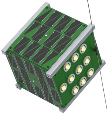
This paper is meant to be a guide and a reference to new and old members alike who wish to know about, understand, and improve on the decisions made and processes implemented to build the current solar panels. The following paragraphs in the introduction will lay out background information on solar panels and cube satellites. This entire document was written with the idea that the reader will be able to follow the decisions made to construct the solar panels and then with this knowledge find areas of the project for improvement....

Publisher: iSAT Group

iSAT Group

We are a student group at Brown University working to build a low-cost, open-source CubeSat, EQUiSat.

Providence, Rhode Island, USA

Other

A System Level Electrostatic Discharge Protection Modeling Methodology for Time Domain Analysis.

Apr 03, 2014 | Nicolas Monnereau, Fabrice Caignet, David Trémouilles, Nicolas Nolhier, Marise Bafleur.

A system level modeling methodology is presented and validated on a simple case. It allows precise simulations of electrostatic discharge (ESD) stress propagation on a printed circuit board (PCB). The proposed model includes the integrated circuit (IC) ESD protection network, IC package, PCB lines, passives components, and externals elements. The impact of an external component on the ESD propagation paths into an IC is demonstrated. Resulting current and voltage waveforms are analyzed to highlight the interactions between all the elements of an operating PCB. A precise measurement technique was designed and used to compare with the simulation results. The model proposed in this paper is able to predict, with good accuracy, the propagation of currents and voltages into the whole system during ESD stress. It might be used to understand why failures occur and how to fix them with the most suitable solution....

Publisher: Institute of Electrical and Electronics Engineers (IEEE)

Institute of Electrical and Electronics Engineers (IEEE)

IEEE is the world's largest professional association dedicated to advancing technological innovation and excellence for the benefit of humanity.

Piscataway, New Jersey, USA

Association / Non-Profit

Cleaning PCB's in Electronics - Understanding Today's Needs.

Mar 27, 2014 | P.J. Duchi, Anne-Marie Laugt, Marie Verdier, G.Aabidh.

Because of the phase out of CFC's and HCFC's, standard solder pastes and fluxes evolved from RA and RMA fluxes, to No-Clean, to low residue No-Clean, to very low residue No-Clean. Many companies came out with their cleaning solutions, aqueous and semi-aqueous, with each product release being more innovative than the previous one. Unfortunately for most of the suppliers of cleaners, two other trends appeared; lead-free soldering and the progressive miniaturization of electronic devices....

Publisher: Inventec Performance Chemicals

Inventec Performance Chemicals

Inventec, one of Europe's leading Performance Chemicals companies, is the high-tech industries business of the Dehon Group

Vincennes , France

Manufacturer

PCB Surface Finishes & Cost Effective Pb Free Assembly Materials

Mar 27, 2014 | Richard Puthota Director – Business Development & CTS India & Africa, Cookson Electronics

The surface finish you select will have a large influence on quality, reliability and cost. It is a complex decision that impacts many areas of the business. Select a finish that optimal for the business (and not just one function). Know that there are engineering tricks to improve on weak areas of each finish. Stay current in this field because new developments continue to be made....

Publisher: Cookson Electronics

Cookson Electronics

Leading materials science company that provides high performance materials, chemistry and technology solutions to the electronics and surface finishing industries worldwide.

Lakeville, Minnesota, USA

Manufacturer

Data Bus Components - The Communication System that Helps in Transferring Data

Mar 27, 2014 | Joe Faruqui

Data bus in computer terminology is a communication system that helps in transferring data between components within a computer, or between separate computers. Know more about data bus components and advancements in data bus technology by reading this article....

Publisher: Just Connectors

Just Connectors

Just Connectors - Supplier of high-grade connectors and interconnects parts

Anaheim, California, USA

Distributor, Other

Today's Vapor Phase Soldering An Optimized Reflow Technology for Lead Free Soldering

Mar 20, 2014 | Dipl.-Ing. Helmut Leicht; Andreas Thumm - IBL-Löttechnik GmbH.

In the beginning of SMT, Vapor Phase Soldering was the preferred reflow soldering technology because of its excellent heat transfer capabilities. There were also some disadvantages like fast temperature rise, nearly no influence on the temperature profiles and high costs. So the use of Vapor Phase Soldering was reduced to special applications with high mass or complex boards in low numbers (e.g. for military or aerospace use)....

Publisher: IBL - Löttechnik GmbH

IBL - Löttechnik GmbH

Manufacturer of vapor phase soldering systems and associated products since 1985.

Königsbrunn, Germany

Manufacturer

Stencil Design Guidelines for Electronics Assembly Technologies.

Mar 13, 2014 | Budapest University of Technology and Economics Department of Electronics Technology

A student competition paper at Budapest University of Technology And Economics, Department of Electronics Technology gives background, covers stencil design and discusses stencils intended for pin in paste application. The stencil applied for depositing the solder paste is a thin, 75–200 µm thick metal foil, on which apertures are formed according to the solder pads on the printed circuit board. Stencil printing provides a fast, mass solder paste deposition process; relatively expensive, appropriate and recommended for mass production....

Publisher: Budapest University of Technology and Economics

Budapest University of Technology and Economics

BME is considered the world's oldest Institute of Technology which has university rank and structure. It was the first institute in Europe to train engineers at university level.

Budapest, Hungary

Research Institute / Laboratory / School

Investigation and Development of Tin-Lead and Lead-Free Solder Pastes to Reduce the Head-In-Pillow Component Soldering Defect.

Mar 06, 2014 | Jasbir Bath, Roberto Garcia - Christopher Associates Inc. Noriyoshi Uchida, Hajime Takahashi, Gordon Clark, Manabu Itoh - Koki Solder

Over the last few years, there has been an increase in the rate of Head-in-Pillow component soldering defects which interrupts the merger of the BGA/CSP component solder spheres with the molten solder paste during reflow. The issue has occurred across a broad segment of industries including consumer, telecom and military. There are many reasons for this issue such as warpage issues of the component or board, ball co-planarity issues for BGA/CSP components and non-wetting of the component based on contamination or excessive oxidation of the component coating. The issue has been found to occur not only on lead-free soldered assemblies where the increased soldering temperatures may give rise to increase component/board warpage but also on tin-lead soldered assemblies....

Publisher: Christopher Associates Inc.

Christopher Associates Inc.

A pioneering supplier and distributor to the electronics and chemical processing industries.

Santa Ana, California, USA

Manufacturer

A Novel High Thermal Conductive Underfill For Flip Chip Appliation

Feb 27, 2014 | Dr. Mary Liu and Dr. Wusheng Yin

Silicon dioxide is normally used as filler in underfill. The thermal conductivity of underfill is less than 1 w/mk, which is not able to meet the current flip chip application requirements such as 3D stacked multi-chips packaging. No matter which direction the heat will be dissipated through PCB or chip, the heat has to pass through the underfill in 3D stacked chips. Therefore the increase of thermal conductivity of underfill can significantly enhance the reliability of electronic devices, particularly in 3D package devices...

Publisher: YINCAE Advanced Materials, LLC.

YINCAE Advanced Materials, LLC.

Yincae Advanced Materials, LLC is a developer, manufacturer, and supplier of high performance coatings, adhesives, electronic and optoelectronic materials.

Albany, New York, USA

Manufacturer

Screening for Counterfeit Electronic Parts

Feb 20, 2014 | Bhanu Sood and Diganta Das

In this chapter, we discuss the type of parts used to create counterfeits and the defects/degradations inherent in these parts due to the nature of the sources they come from, proposed inspection standards, and limitations of these standards. The processes used to modify the packaging of these parts to create counterfeits are then discussed along with the traces left behind from each of the processes. We then present a systematic methodology for detecting signs of possible part modifications to determine the risk of a part or part lot being counterfeit....

Publisher: CALCE Center for Advanced Life Cycle Engineering

CALCE Center for Advanced Life Cycle Engineering

The largest electronic products research center focused on electronics reliability, is dedicated to providing a knowledge and resource base to support the development of competitive electronic components, products and systems.

College Park, Maryland, USA

Consultant / Service Provider, Training Provider

Why Signal Always Be Loss in a High Speed, High Frequency Transmission Line

Feb 13, 2014 | Albert Chen.

The high speed transmission applications in the electronic product become inevitable developing trend. The signal integrity becomes the most important issue in the electronics industry. The material suppliers, PCB manufacturers, OEM designers commonly face the serious issue "how to keep signal integrity operated in the high speed transmission" for the modern electronic application nowadays...

Publisher: Elite Material Co., Ltd.

Elite Material Co., Ltd.

Manufacturer of base materials for the PCB industry. Our main products are copper clad laminates (CCL), prepregs (PP) and Mass Lamination boards (Mass Lam PCBs).

Guanyin Township, Taiwan

Manufacturer

Understanding SIR

Feb 06, 2014 | Chris Nash, Technical Support Engineer, Eric Bastow, Senior Technical Support Engineer; Indium Corporation.

Many electronics manufacturers perform SIR testing to evaluate solder materials and sometimes the results they obtain differ significantly from those stated by the solder material provider. The difference in the results is typically the result of SIR coupon preparation. This paper will discuss the issue of SIR coupon preparation, board cleaning techniques, and how board cleanliness directly affects SIR results....

Publisher: Indium Corporation

Indium Corporation

Solder pastes, solder preforms, solder spheres, soldering fluxes, electrically-conductive adhesives. All alloys: tin-lead, lead-free, indium alloys, and more.

Utica, New York, USA

Manufacturer

per page.

Pages: 1 2 3 4 5 6 7 8 9 10 11 12 13 14 15 16 17 18 19 20 21 22 23 24 25 26 27 28 29 30 31 32 33 34 35 36 37 38

Win Source Online Electronic parts

Circuit Board, PCB Assembly & electronics manufacturing service provider