Nov 05, 2019
There are two wire bonding processes that are used, Thermosonic (T/S) Gold Ball Wire Bonding and Ultrasonic (U/S) Aluminum Wedge Wire Bonding. Approximately 90% of all IC Assembly in Semiconductor Packages is manufactured using Gold Ball Bonding process, while Aluminum Wedge Bonding is used to produce about 10% of other Wire Bonding requirements on Printed Circuit Boards (PCB), Printed Circuit Flex (PCF) and other Packages.
Gold Ball Bonding
In this technique, wire is passed through a hollow capillary and a Negative Electronic Flame Off (EFO) system is used to melt a small portion of the molten gold wire forming a ball as the wire material solidifies. The ball is pressed to the first bonding pad on the die (IC) with sufficient force to cause deformation and interdiffusion of the wire and the underlying metallization, which ensures the contact between the two metal surfaces and form the first bond (ball bond) on the IC. The capillary is then raised and moved to the second bond site creating a wire loop, deforming the wire against the bonding pad and thus creating a second wedge bond on the substrate. Then the wire clamp is closed, and the capillary is raised once again, breaking the wire just above the wedge, and exact wire length is left for EFO to form a new ball to begin bonding the next wire.
-“Omnidirectional” wire bonding process – the wire can go in any direction from the top of the ball on the first bond to the second bond on the substrate.
-Requires High Temperature of 150C on the substrate or package during wire bonding.
-Gold wire diameter of 0.7mil/18um, 0.8mil/20um, 1.0mil/25um, 1.25mil/32um, 1.5mil/38um and 2.0mil/50um.
-Minimum Wire Bond pitch of 45um.
-PCB Electrolytic Gold Plating per MIL-G-4-45204C: Purity: Type III, 99.9% minimum gold, Grade A: 90 Knoop maximum hardness, Class 1: 30-50 uinches (0.75-1.25 microns) of soft bondable gold.
-PCB Gold Plating: ENEPIG (Electroless Nickel, Electroless Palladium, Immersion Gold. 120-200 uinches (3 – 5 microns) of Nickel, 3-6 uinches (0.08 – 0.15 microns) of Palladium, 3-6 uinches (0.08 – 0.15 microns) of Gold.
-Substrate/ Package limited to 2.2” (56mm) X-axis x 3.0” (76mm) Y-axis.
-Ball size is approximately 2 to 3 times the wire diameter.
-Bond size should not exceed 75% of the IC pad size.
-Loop heights of 150um – 200um are now common, minimum 100um.
-Loop length should be less than 100 times the wire diameter.
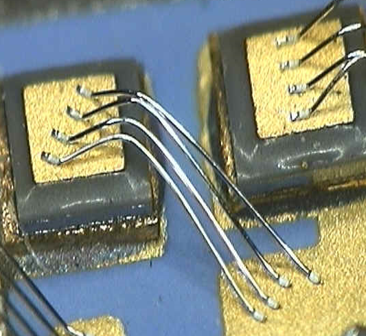
Aluminum Wedge Bonding
Wedge bonding was name based on the shape of its bonding tool. In this wire bonding technique the wire is fed at angle usually 30-60 degree angles (typical 45 degree angle) from the horizontal bonding surface through a hole in the back of a bonding wedge tool. Normally, forward bonding is preferred, i.e. the first bond on the die (IC) and the second bond on the substrate or package. The wedge tool descends on the IC bond pad, the wire is pinned against the pad surface and an Ultrasonic (U/S) first bond is performed. Next, the wedge tool rises and executes a motion to create a desired loop shape in the direction of the second bond, and then the wedge tool descends making the second bond on the substrate or package. Then the wire clamp is closed to break the wire while machine bonding force is maintained on the second bond (clamp tear).
Wedge bonding technique can be used for both Aluminum wire and Gold wire bonding applications. The principle difference between the two processes is that the aluminum wire is bonding in an Ultrasonic (U/S) bonding process at 25C (room temperature), whereas gold wire is performed through a Thermosonic (T/S) bonding process with a high temperature of 150C on the substrate or package.
-“Unidirectional” wire bonding process – the wire bond foot on the IC is always on the direction of the wire to the second bond, sometimes creating potential shorts on corner wire bonds for fine pitch applications with small bond pads on the IC.
-Requires Room Temperature of 25C on the substrate or package during wire bonding.
-Aluminum wire diameter of 0.7mil/18um, 0.8mil/20um, 1.0mil/25um, 1.25mil/32um, 1.5mil/38um and 2.0mil/50um.
-Minimum Wire Bond Pitch of 45um.
-PCB Gold Plating: ENIG (Electroless Nickel, Immersion Gold. 120-200 uinches (3 – 5 microns) of Nickel, 3-6 uinches (0.08 – 0.15 microns) of Gold.
-Substrate or Package up to 10.0” (250mm) X-axis x 8.0” (200mm) Y-axis.
-Wedge bond (foot) is approximately 1.2 to 2.5 times the wire diameter in width, and less than 1.5 to 3.0 times the wire diameter in length.
-Bond size should not exceed 75% of the IC pad size.
-Loop heights of 150um – 200um are now common, minimum 100um.
-Loop length should be less than 100 times the wire diameter.

Plasma Cleaning
To ensure bondability and reliability of the wire bonds, one of the critical conditions is that the bonding surface must be free of any organic contaminants. Therefore cleaning is an important process before wire bonding.
Plasma cleaning technique employs a high power radio frequency (RF) source to convert inert gas used into plasma, the high velocity of gas ions bombard the bonding surface and sputter off contaminants from the bonding surface by combining the contamination molecules, or physically breaking apart the contamination molecules. In most cases, the gas ionized is Oxygen, Argon, and Nitrogen.

Metallurgical Systems (Au or Al Wire to IC Bond Pads)
In wire bonding process, different pad metallizations are used on the IC chip, depending on the production requirements. Therefore, different metallurgical systems can be formed with different reliability behaviors. The typical metallurgical systems are:
Au Wire to Au Bond Pads.
Gold wire bonded to a gold bond pad is the most reliable wire bonding process because the bond is not subject to interface corrosion, intermetallic formation, or other bond degrading conditions.
Au Wire to Al Bond Pads.
Gold wire bonded to an aluminum pad is the most commonly used wire bonding process.
Al Wire to Au Bond Pads.
Not recommended because of reliability concerns.
Al Wire to Al Bond Pads.
Aluminum wire bonded to an aluminum bond pad is extremely reliable because the bond is not subject to interface corrosion, intermetallic formation, or other bond degrading conditions.